Materials Innovations
Full Html
Vol 2 Issue 6
Two-dimensional Materials based Printed Photodetectors
Pages: 160-175
Doi: 10.54738/MI.2022.2602
Doi URL: http://doi.org/10.54738/MI.2022.2602
Ayaz Ali ?? 1 , Nardin Avishan 2 , Shahnawaz Shah 3 , Ayaz Ali Memon 4 , Yaqoob Khan 5
1 Department of Electronic Engineering, Faculty of Engineering and Technology, University of Sindh, Jamshoro, 76080, Pakistan
2 Micro and Nanotechnology Program, Graduate School of Natural and Applied Sciences, Middle East Technical University, Ankara, 06800, Turkey
3 Department of Telecommunication Engineering, Faculty of Engineering and Technology, University of Sindh, Jamshoro, 76080, Pakistan
4 National Center of Excellence in Analytical Chemistry, University of Sindh, Jamshoro, 76080, Pakistan
5 Department of Metallurgical and Materials Engineering, Middle East Technical University (METU), Ankara , 06800, Turkey
Two-dimensional (2D) materials offer several unique advantages for high-performance light detection including fast response, high responsivity, broadband response and relatively low noise levels. 2D materials integrated photodetectors often use chemical vapor deposition grown materials, which despite their good quality are relatively high cost and not easily scalable. 2D materials based inks, fabricated through liquid phase exfoliation of bulk crystals, are attractive alternatives due to their low cost, ease of processing and scalable production. Combined with these advantages, mature printing methods available for 2D inks allow large scale electronic device fabrication for a variety of high performance applications including energy storage, solar cells, photodetectors, etc. In this review, we summarize production of 2D materials based inks, their printing methods, and applications for high performance photodetection.
Keywords
2D materials, Photodetectors, Printed, Inks
Photodetectors (PDs) yield electrical output when exposed to the light. PDs attract considerable interest from academia and the industry. In industry, PDs have found applications in variety of area including image sensing, telecommunication, chemical sensing, biological sensing, safety, and environment.1, 2, 3, 4, 5 Depending on the photosensitive materials used, PDs can operate in the range extending from X-rays to Terahertz. Silicon (Si) is the material of choice for photo detection due to its availability, cost, optical properties and mature fabrication technology. 6, 7 However, Si cannot operate for the wavelengths larger than near infrared (NIR) due to its bandgap. For wavelengths beyond IR, narrow bandgap materials such as Ge, III-IV semiconductor have been used, however, direct growth of these materials on Si chips is challenging due to different lattice structures. 8, 9Moreover, there are no bulk materials available, which can work in truly a broad band range.
With advent of two-dimensional materials, new avenues have opened for the10, 11 Furthermore, due to their atomic thickness and strong mechanical properties, 2D materials are very attractive for flexible PDs, especially for bio and health related applications. 12 ?Due to these unique set of properties, 2D materials based photodetectors are recent focus of scientific research. Various 2D materials including Gr, boron nitride (BN), transition metal dichalcogenides (TMDCs), MXenes, and metal oxides have been reported for the photodetection with performance parameters outperforming conventional semiconductor based PDs. 13, 14, 15, 16 2D materials also operate in broadband, and also offer range of bandgaps suitable for narrow band wavelength detections. 14, 17 Due to the dangling bond-free surfaces, 2D materials can also be interfaced with the bulk semiconductors to form atomically thin heterojunctions, which allow fast and sensitive photodetection compared to pure 2D based PDs. Most of the reported 2D materials base PDs are based on either mechanically exfoliated or chemical vapor deposition (CVD) grown 2D materials. These methods, though produce good quality 2D materials, are not easily scalable. Hence, most of the high performance 2D materials based PD demonstrations are on the lab scale and haven’t been commercialized yet.
Liquid phase exfoliated (LPE) 2D materials have low quality, but can be produced on large scale. Methods for LPE exfoliated materials can also be modified to synthesize stable inks which can be easily printed controllably into electronic devices. 18, 19, 20 Hence, 2D inks have large potential for large-scale commercial printed electronics, especially for PDs. In this review, we summarize recent developments on 2D ink development/formulation and their use for developing high performance printed PDs.
2D materials can be synthesized by bottom-up or top-down approaches. While bottom-up approaches, such as CVD produce high quality 2D materials, but high cost (due to large energy consumption due to high temperature involvement) and lack of scalability limit their applications. LPE, which is a top-down approach and involves exfoliation of mono and few layers of 2D materials from bulk solids, is a low cost and easily scalable method for 2D production. 21 As product of LFE exfoliation is 2D material dispersed in a solvent, such dispersions, if properly stabilized in a suitable solvent, can be converted into printable functional inks for various applications. 18 Large scale ink formation, printing, and exciting physical/optical properties of 2D inks make them particularly suitable for printable optoelectronic devices such as photodetectors, light emitting diodes, and solar cells. 22, 23
During LPE, layers of bulk materials are delaminated by overcoming week inter-layer van der Waals (vdW) forces, by using various mechanisms and techniques (Figure 1). These techniques involve sonication, intercalation of ions/electrochemical exfoliation, or shear exfoliation. In sonication, ultrasonic waves produce solvent bubbles, which first expand and the burst to producer micro jets, which help delaminate the layers. However, high energy micro jets can also damage the crystal structure of the layers, and in extreme cases, when sonication is carried out for longer times and at high energy for large/fast production, flakes are fragmented and final size of the flakes reduces. 24 Hence, there is a trade-off between the quality of 2D crystal and the scale of production for sonication assisted LPE. Shear exfoliation of 2D materials was initially thought to be slow process 25, however, in 2014, Paton et al., reported hundreds of liters of defect free graphene using shear exfoliation. 26 Layers started exfoliating only when the local shear force exceeded 104/s. This method was also demonstrated to be applicable for other 2D materials such as hBN and molybdenum disulfide (MoS2). Intercalation of ions is another method to exfoliated the bulk vdW materials. Surprisingly, intercalation method was used as early as 1986 to exfoliate the MoS2 monolayers 27, and recently has been used to exfoliate variety of other 2D materials as well. In this method small ionic species such as Li+, K+, Na+ are electrochemically intercalated between the layers, which expands the layered compounds and weaken the inter-layer vdW forces by increasing the distance between the layers; and subsequently, mild stirring can exfoliate the layers of these intercalated layered compounds. 28 This method is suitable for production of large flake size of 2D materials. However, as very obvious, intercalated ions can change the properties of exfoliated layer through physical/chemical interaction. For example, MoS2, when intercalated with Li+ ions can change to metallic phase form semiconducting phase due to change of its structure form trigonal prismatic phase to metastable octahedral phase. 29 For layered oxide materials, which contains interlayer cations (such as e.g. K+, Rb+, Cs+), these cations can be replaced with bulky organic cations (such as tetrabutylammonium (TBA+), which lead to swelling and consequent exfoliation mono and few layers of oxides. 28 Compared to electrochemical exfoliation in water, use of organic solvent, though less environmentally friendly, produces high quality 2D materials. 30, 31
LPE 2D materials have wide range of size and thickness, even some times contain big chunks of non-exfoliated bulk materials. To obtain a narrow size and thickness distribution, techniques such as ultra-centrifugation in uniform or gradient media is performed to separate small flakes form large flakes. 32 Another problem is re-aggregation of the layers which can compromise the physical properties of 2D materials by invoking inter-layer coupling. Suspensions of exfoliated materials can be stabilized via adding polymers, surfactants or organic molecules such as pyrene. Surfactant molecules absorb on the 2D surface and satisfy their vdW charge. These surfactants coated 2d layers repel other coated layers and prevent the re-aggregation. Both ionic (sodium cholate and sodium deoxycholate) 33, 34, 35 and non-ionic surfactants (Triton-X, Tween and Brij series, and polymers such as sodium carboxymethylcellulose (Na-CMC), polyvinylpyrrolidone (PVP) and ethyl cellulose) 28, 36, 37 have been used for this purpose. Compositions (pigment, binder, additives) and properties (viscosity) of inks required for various printing techniques are presented in Table 1. Silent features/advantgaes of rprintign technologies are also presented.
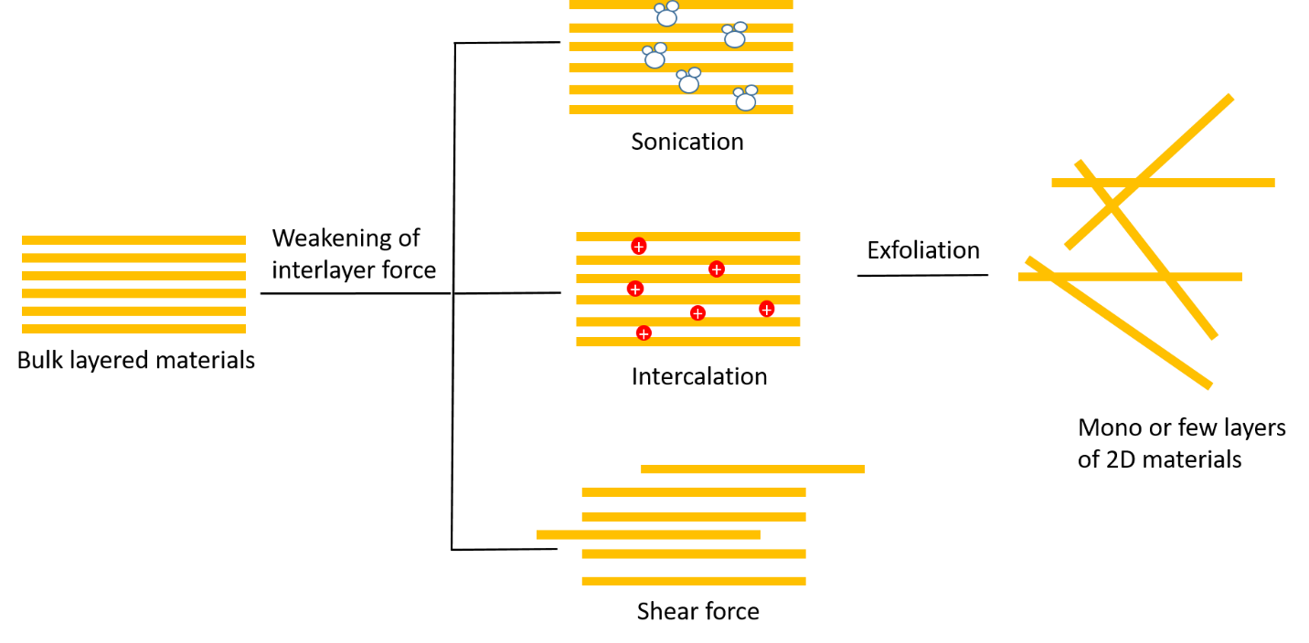
Figure 1: Schematics of liquid phase exfoliation techniques for obtaining mono or few layers of 2D materials from bulk materials.
All the methods used for conventional ink printing can be used for 2D materials based inks. Before ink deposition with a particular technique, ink properties need to be optimized for that particular technique and the substrate. Ink properties like color, viscosity, conductivity, and spread can be controlled by choice of ink material, solvent, binder and surfactants. Choice of printing technique is also dictated by production scale as some techniques are suitable for small scale production and some for the large scale.
Various printing techniques employed for 2D materials based techniques include drop casting, spray coating, spin coating, screen printing, Inkjet printing, Gravure and Flexo printing. Details of these techniques are described below.
Table 1: Typical composition of Ink prepared for different printing processes. Some data taken from ref. 20
|
Printing Technique |
Pigment (wt.%) |
Binder (wt.%) |
Solvent (wt.%) |
Additive (wt.%) |
Viscosity (mPa. S) |
Features |
|
Inkjet |
5–10 |
5–20 |
65–95 |
1–5 |
4–30 |
No contact, Digital, low ink, high resolution |
|
Screen |
12–20 |
45–65 |
20–30 |
1–5 |
1k–10k |
Low resolution, Contact based. Simple, robust |
|
Gravure |
12–17 |
20–35 |
60–65 |
1–2 |
100–1k |
Need large quality of inks, scalable |
|
Flexo |
12–17 |
40–45 |
25–45 |
1–5 |
1k–2k |
Need large quality of inks, scalable |
Drop casting is the simplest printing process, where ink is dropped on the substrate and then the let the solvent dry (Figure 2). Process is low cost, scalable and is already used in industry. However, using this method selective printing with good resolution is not possible. This method is suitable for large films. However, the uniformity of the films (thickness, structure) using this method is not good. 38 To improve the process, several modifications have been made, which include azeotrpoic mixtures, inter gas purging, and solvent saturation environment. 39, 40, 41
Spray coating is a highly efficient, fast, simple and high density printing techniques for the functional inks. In this method, ink is simply sprayed on the substrate using a sprayer. For spray coating binder are also often required to achieve better dispersion of the ink material and also to ensure the optimization of viscosity for uniform coating. 42, 43 One drawback of spray coating is low resolution of printed patterns as it is difficult to spray the inks on the targeted area of substrate.
Spin coating is a standard process in electronic industry for thin film deposition of various materials from the solutions. Same process has been used for 2D inks printing. In this technique, ink is dropped on a substrate spinning at a certain speed (Figure 2). Thickness of the deposited film is controlled by spinning time, speed, velocity, and viscosity of the ink. 44 This technique is most suitable for high quality and ultra-thin films. However, like drop casting, it is not possible to selectively deposit the ink on the substrate. 45
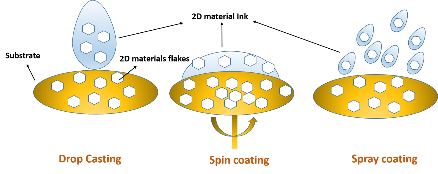
Figure 2: Schematics of drop casting, spin coating and spray coating techniques for 2D materials ink printing.
Screen printing is also a straight forward printing method, where a porous mesh of fabric, silk, synthetic fibres or metal threads is used to transfer the ink to the substrate except the areas made impermeable to the ink by using blocking stencils. 46, 47 For screen printing, high viscosity inks are required, so that the integrity of the patterns is retained. As most 2D inks are low viscosity, polymer binders such as PVP, PANI, PVP and ethyl cellulose are added to the ink to achieve the high viscosity ink. 48, 49, 50 However, in some processes, in the post-printing, to get rid of binder, high temperature processing is required which can affect the deposited film. For example, Zhang et al., designed rGO ink in terpineol with ethyl cellulose as the ink binder for deposition of counter electrodes for dye sensitized solar cells. 48 However, post printing heating at 400 °C to get rid of binder adversely effected the binding of the film to the substrate. For screen printing, binder free, high viscosity 2D inks are required so that post-printing treatments can be avoided.
Inkjet printing is a non-contact, digital printing (printing pattern is designed by computer and also controlled via computer) technique, which is most suitable for lab scale printing, where a precise printing of structure on small scale is required. 51 Inkjet technique can be further divided in two techniques, i.e., continuous and drop on demand. In continuous process, ink is continuously generated and jetted, however, in drop on demand, drops are generated when demanded and process is controlled by piezoelectric. 20 Other modifications of inkjet printing, to improve homogeneity and resolution, are electrohydrodynamic-jet and aerosol-jet printing. 52, 53. Relation between ink jetting and the ink properties is given by following relationship,
Z=1Oh=ργαη
Where γ, ρ and η are the viscosity, density and surface tension of the ink, respectively, and a is the nozzle diameter. Z is a dimensionless number and Ohnesorge (Oh) is its inverse. 54 Generally, a Z number between 1-14 is deemed appropriate for stable printing, though stable printing for Z number beyond mentioned range are also reported. As low viscosity inks are generally used for the inkjet printing, coffee ring effect (accumulation of greater amount of materials at borders) is usually observed after drying, which can be solved by using mixture of solvents or choosing high boiling point solvents. 55, 56
Both gravure and flexographic printing processes are roll to roll (R2R) and hence can be used for high speed printing (upto 1000 m/min). In Gravure printing, patterns that are to be printed, are engraved into the roller. 57Metal gravure roller rolls in the fluid ink and doctor blade wipes the excess inks from the non-patterned parts of the roller. When the substrate passes through between the gravure roller and the impression roller, inks and patterns are transferred to the substrate. 57, 58 Smoothness and quality of printing process depends on three forces, i.e., cohesive force inside the ink (FCI), adhesive force on cell (FAC), and adhesive force on the substrate (FAS). If FAS > FAC > FCI, then successful printing can be achieved, otherwise ink will not transfer to the substrate properly.
In contrast, flexographic printing is a relief process, where pattern is embossed in relief on a cylinder. After being inked, pattern is impressed on the substrate. In flexographic printing, the amount of ink a cell absorbs is of critical importance for the printing process. 57 Inks used for both gravure and flexographic printing are of medium viscosity (100–1000 mPa s). 59, 60 Relatively, large amount of ink is required for both of these processes. Since both of these processes are high speed, so a low boiling point solvent is required, so that it can evaporate easily and drying process becomes fast. 60
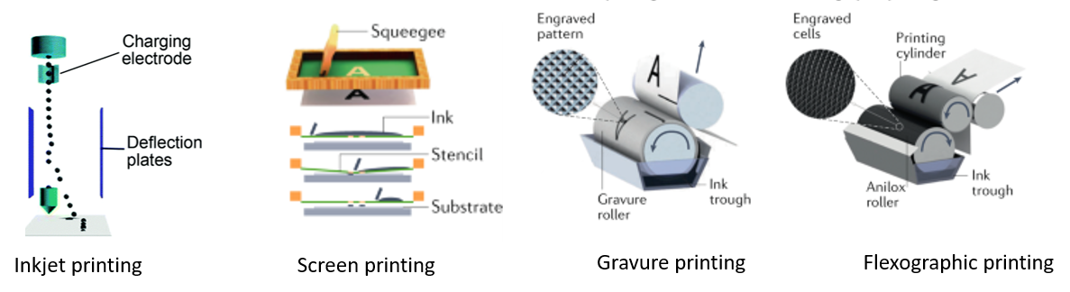
Figure 3: Schematics of Inkjet printing, screen printing, gravure printing, and flexographic printing techniques for 2D materials ink printing. 20 Copyright RSC, 2018. Reproduced with permission.
Seo et al., reported inkjet-printed MoS2/Gr photodetectors. MoS2 acted as the active materials, while Gr acted as electrodes. MoS2 powder and ethyl cellulose (EC) mixture was shear mixed together to achieve MoS2exfoliation. 61 Obtained EC/MoS2 mixture was then re-dispersed in a cyclohexanone/terpineol (CT) solvent system to optimize the viscosity of the ink for inkjet printing process. Similarly, Gr/EC mixture was dispersed in the cyclohexanone/terpineol/diethylene glycol methyl ether solvent system to obtain the Gr inks. PDs were inkjet printed on the glass and polyimide (PI) substrate (Figure 4). After printing, samples were annealed at 400 °C to decompose the EC so that the contact between 2D flakes improves which will subsequently improve the conductivity. Samples were annealed thermally (Figure 5) and with light (photonic annealing, Figure 4). Photonic annealing is suitable for the substrate which are sensitive to thermal treatment (such as plastic substrates). MoS2/Gr/PI devices were photonically annealed (PA) while MoS2/Gr/Glass devices were thermally annealed (TA).
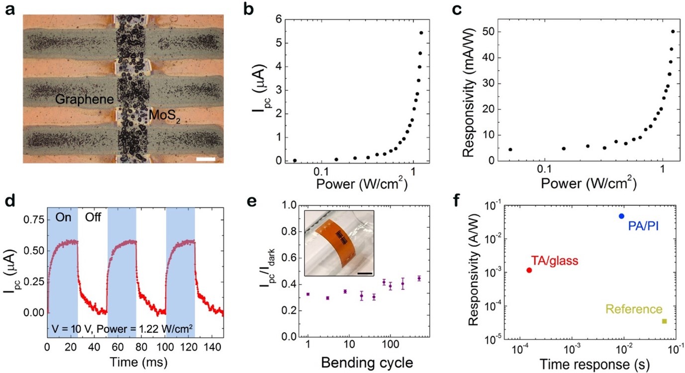
Figure 4: Fully printed MoS2-Gr photodetectors prepared with photonic annealing. (a) Optical microscopy image of the inkjet-printed photodetector on PI after photonic annealing, with a vertical MoS2/EC channel and horizontal graphene/EC electrodes. The scale bar is 100 μm. (b, c) Photocurrent and responsivity as a function of laser intensity at a bias voltage of 40 V. (d) Temporal response showing current modulation as the laser is switched on and off at a bias voltage of 10 V. (e) Bending test over 500 cycles showing invariant sensitivity. Inset: photograph of the flexible MoS2-Gr device. The scale bar is 3 mm. (f) Comparison of photodetector characteristics from MoS2-Gr TA on glass (red), MoS2-Gr PA on PI (blue), and literature precedent for MoS2–Ag thermally annealed on SiO2/Si. (14) 61 Copyright ACS, 2019. Reproduced with permission.
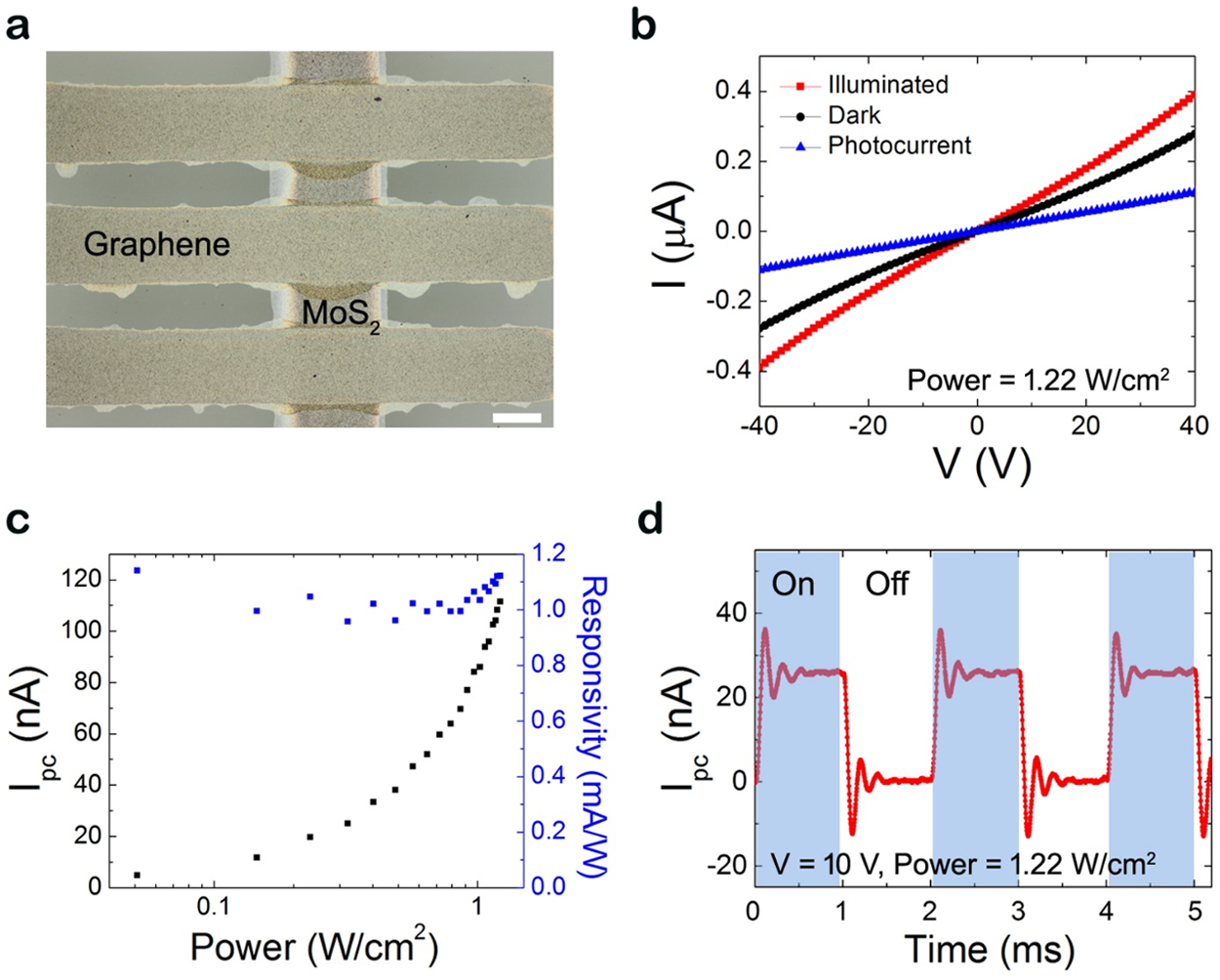
Figure 5: Fully printed MoS2-Gr photodetectors prepared with thermal annealing. (a) Optical microscopy image of the MoS2/EC channel (vertical line) and graphene/EC electrodes (horizontal lines) after annealing. The scale bar is 100 μm. (b) Current−voltage curves of a MoS2-Gr TA photodetector showing the dark and illuminated (λ = 515.6 nm, laser intensity = 0.6 W/cm2) currents, and the corresponding photocurrent. (c) Photocurrent and responsivity as a function of intensity at a bias voltage of 40 V. (d) Temporal response showing current modulation as the laser is switched on and off at a bias voltage of 10 V. 61 Copyright ACS, 2019. Reproduced with permission.
At λ = 515.6 nm, responsivity value of ∼1 mA/W for the MoS2-Gr TA and response time of less than 150 μs was observed for thermally annealed MoS2/Gr/Glass devices. For MoS2/Gr/PI photonically annealed devices responsivity value exceeding 50 mA/W was observed. Response of these devices was different from thermally annealed devices particularly a superlinear intensity dependence for the photocurrent and a slower photoresponse time. This was attributed to presence of pores in MoS2 film due to rapid evaporation of solvent under the light. Presence of pores was responsible for low electrical and thermal conductivity. PDs printed on PI were also flexible and exhibited stable performance upto 500 bending cycles. 61
In a similar work, inks of Gr and MoS2 were fabricated by exfoliating their bulk counterparts in a cyclohexanone/terpineol (CT) mixture. 62 CE was also added in the mixture as a binder. The mixture was centrifuged to separate larger flakes. In the final dispersion, Gr and MoS2 powders were added to further increase the concentration of the inks. MoS2 was inkjet printed on PI substrates with Mo contact, as shown in Figure 6. samples were annealetd at 300 °C before printing of Gr electrodes on top. Device was annealed again after Gr printing at 300 °C. After evaporation of the solvents thickness of Gr and MoS2 films decreased form ~ 0.8 μm and 1.6 μm to ~ 0.4 μm and 0.9 μm, respectively. PDs exhibited a good sub-linear behavior with light intensity (F), meaning the less-trap density of the carriers, which is encouraging for the printed photodetectors. Responsivity, Detectivity, and speed of the photodetectors at 550 nm wavelength was recorded as 0.11A/W, ~ 1.7 × 10¹⁰ jones and 1.3 s, respectively (Figure 7).
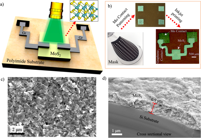
Figure 6: Schematics of the flexible MoS2-graphene heterostructure device. Inset shows the layered 2D structure of MoS2. (b) The device fabrication steps to form the inkjet-printed MoS2-graphene heterostructure photodetector bridging the Mo electrodes used for contacts. (c) The SEM image of the printed MoS2 on a Si substrate. (d) Cross-sectional SEM image of the printed MoS2 layer on a Si substrate. 62 Copyright Springer, 2022. Reproduced with permission.
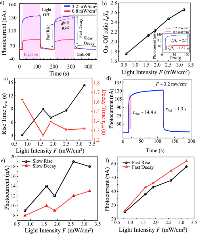
Figure 7: The Ip response to a periodic llumination source at two different F (~ 0.8 and 3.2 mW/cm2) as a function of time. (b) Ip/Id with different illuminating F. The inset is showing the Ip/Id to F ~ 0.8 mW/cm2 and 3.2 mW/cm2. (c) The τrise and τfall of Ip plotted against F. (d) The Ip response to a single-step illumination, which shows the τrise ~ 14.4 s and τfall ~ 1.3 s at F ~ 3.2 mW/cm2. (e) The slow rise and decay of the Ip versus F (f) The fast rise and decay of the Ip plotted against F. 62 Copyright Springer, 2022. Reproduced with permission.
In another study, an almost similar ink preparation method was adopted for Gr and MoS2 inks. Biocompatible 2D graphene-MoS2 photodetectors on a flexible polyimide substrate were fabricated by using inkjet printing with a responsivity value of ∼ 0.30 A/W at room temperature. A strong photocurrent value of 1.16 μA was observed for a bending curvature of utpo 0.262 cm-1. 63 A study by Hossain et al on the Gr and MoS2 inks used for inkjet printing the biocompatible PDS shows that both of the inks prepared in the CT has better photocurrent compared to those prepared in the IPA and N-Methyl-2-pyrrolidone (NMP). So, it seems that the CT is a better solvent for inkjet printing the Gr and MoS2 inks. Moreover, both of these inks have also shown biocompatibility without any obvious damage to the cells. 64
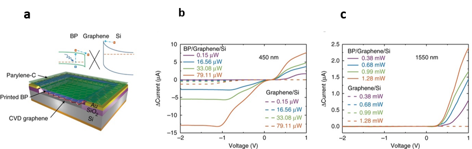
Figure 8: chematic of the BP/graphene/Si Schottky junction photodetector and the device band diagram configuration. Associated current response for f 450 nm and g 1550 nm illumination, the dashed lines show the response of the graphene/Si Schottky junction photodetector without printed BP 55. Copyright Nature Publishing Group, 2017. Reproduced with permission.
Gr/Si-based photodetectors are recently the focus of attention due to their room temperature high-speed operations at a relatively good responsivity. However, the detection wavelength of these PDs is limited to NIR due to the bandgap of Si. However, by coupling Gr/Si structure with other functional materials can broaden the operating wavelength of these photodetectors. Guo et al, have reported black phosphorous (BP) printing on Gr/Si devices to improve the IR response of these PDs. 55 BP is not stable in the ambient 65, hence, its ink formation and stable printing is a challenge. To fabricate the BP ink, BP crystals were dispersed in NMP, CHP, and IPA in a sonication tube, these tubes were filled with nitrogen, sealed and sonicated for 12 h. For ink printing, low boiling pint and low surface tension, hence NMP and CHP (which are high surface tension liquids) solvent-based inks are not suitable for the printing. Hence, the BP flakes from NMP were transferred to IPA through the solvent exchange to prepare BP inks in IPA. 2-butanol (10 vol%) is then added to formulate the ink. To protect BP from ink oxidation, after inkjet printing, BP layers were encapsulated with a parylene-C passivation layer can preserve it against oxidation for > 30 days.
The Figure 8 shows the photocurrent of Gr/Si and BP/Gr/Si devices at 450 nm and 1550 nm excitation laser. At 450 nm Gr/Si has a reverse-biased responsivity of 16 mA/W, while BP/Gr/Si has both forward (164 mA/W) and reverse biased (95 mA/W) responsivity greater than Gr/Si devices. At 1550 nm excitation, Gr/Si devise show no response in reverse or forward bias. However, BP/Gr/Si devices show a ~1.8 mA/W response, demonstrating that BP coating enables the IR response of Gr/Si devices. The enhanced response may be due to improved absorption of light and the charge transfer from BP to Gr, and the photogating effect. Charge transfer to Gr from BP may change its Fermi level and charge transport in Gr/Si Schottky interface. Response speed of the photodetectors was 0.55 ms.
While mostly organic solvents are used for the ink development, these solvents are not environmentally friendly. Xi et al., have developed the WS2 and MoTe2 water-based inks, which avoid the organic solvents. Initial water dispersion of WS2 and MoTe2 were fabricated in the presence of 1-pyrenesulfonic acid sodium salt (PS1) as the exfoliating and stabilizing agent, and then these dispersions were sonicated for 72 h, followed by the centrifugation. 66 MoTe2 and WS2 were then inkjet printed onto the Gr sheet to from WS2/Gr and MoTe2/Gr heterostructures. At 532 nm excitation, 20 mA/W and 2.5 A/W at 532 nm, respectively, Moreover, the inkjet-printed MoTe2/graphene shows a responsivity of 7.7 mA/W at 940 nm, demonstrating their scope for NIR photodetection.
β-InSe inks were fabricated by exfoliating 40 mg of the InSe in IPA by sonicating for 6 h, followed by sedimentation based separation. 30ml of the ink was spray coated on FETs fabricated on a p-type Si chip, while heating on 60 °C. 67 Samples were dried in vacuum overnight and then annealed in argon for 30 min at 300 C. PDs exhibited a high responsivity value of 274 A W−1 @455 nm (Figure 9). One order improvement than previously reported results, and relatively fast response time of 15 ms. High responsivity was attributed to small channel length and better β-InSe coverage. The use of simple spray coating method and environmentally friendly solvents in the fabrication process are important benefits of these type of photodetectors. These photodetectors can also be fabricated on flexible substrates.
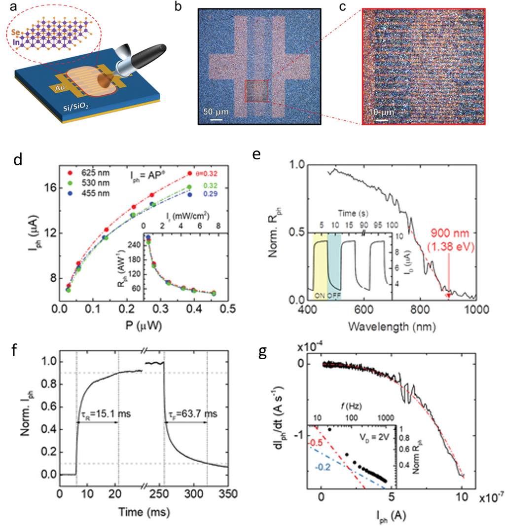
Figure 9: Schematic illustration of the β-InSe photodetector. b) Optical microscope image of the complete photodetector and c) magnified detail of the conducting channel region. a) Photocurrent vs different powers of three different optical wavelengths. The dashed lines represent a power-law fit to the data. The inset plots the photoresponsivity R versus the irradiance I. b) Spectral responsivity of β-InSe photodetector. The inset plots the response to 0.1 Hz pulsed light (530 nm) (c) Detail of photocurrent rise and decay during pulsed (2 Hz) 625 nm light excitation. d) Plot of the time derivative of the photocurrent versus the photocurrent after switching off the light. Inset: Responsivity versus light chopping frequency under illumination at 625 nm. Dashed lines indicate the power laws.67Copyright Wiley, 2020. Reproduced with permission.
Fuad et al., has reported that size selection of flakes in 2D inks (through centrifugation) and controlled mixing of the different 2D materials in the inks can substantially improve the performance of the photodetectors.68They observed that printed photodetectors (printed using electrohydrodynamic (EHD) printing) based on 2D sheets with larger flake size have faster response speed compared to the small size. 2D materials such as WS2and MoS2 have better light absorption but conductivity is low. Mixing these materials with high conductivity 2D materials such as Gr can improve the conductivity of the inks of these materials. But conductivity values of mixed inks beyond a certain range can increase the dark current beyond tolerance limits. Fuad et la, have mixed WS2 and MoS2 with Gr. It was noticed that the content of Gr below the percolation threshold (formation of connecting networks), can significantly improve the photoresponse (up to 40 times, reaching 1.15 A W−1 under blue light) without significantly increasing the dark current. However, beyond the percolation threshold (beyond the critical concentration of Gr), dark current increases significantly which offset the increase in photocurrent. Same strategy of flask size selection and mixing of different 2D materials can also be implemented across the spectrum of 2D materials inks such as phosphorene, MXene, and graphitic carbon nitride.
Using ink printing, Ting et al., have fabricated a more complex heterosructure for photodetection, which allows the wireless photosensing. 69 Near field communication (NFC) tag antenna based on Gr was first screen printed (purple color in Figure 10 ) and was integrated with WS2 based photodetecrtor. WS2 and top Gr was inkjet printed on technical paper (PEL P60) substrate. Gr and WS2 inks were fabricated using sonication followed by centrifugation. At 532 nm incident light, the photo-responsivity of the printed photodetectors were 0.61, 0.46 and 0.41 mA W−1 for devices with 40, 50 and 60 print passes of WS2, respectively, however, the response time was relatively slow.
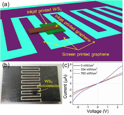
Figure 10: (a) Schematic and (b) optical image of the inkjet printed WS2 photodetector integrated with screen printed graphene meandered line. (c) I–V characteristics of the photodetector device shown in (b). 69 Copyright Institute of Physics, 2020. Reproduced with permission.
Apart from all 2D inks, 2D materials are also combined with other materials (nanoparticles, quantum dots), either during the ink formation or printing process to fabricate the PDs. In one such example, ZnO sol–gel precursor (ZnOPr) and graphene nanoplatelets (GnPs) are mixed into a composite ink for inkjet printing photodetectors with bulk heterojunctions of ZnO/GnP on a heated SiO2/Si substrate.70 Heating of the SiO2/Si wafers at ∼50 °C was found optimal to prevent segregated droplets on the hydrophobic surface of the SiO2/Si substrate during printing. After printing the ZnO/GnP channels, thermal annealing at 350 °C for 2 h was performed for crystallization of ZnO and formation of the ZnO/GnP heterojunctions. The GnP concentration was varied from 0, 5, 20, and 30 mM to evaluate optimal formation of the ZnO/GnP bulk heterojunction nanocomposites based on ultraviolet photoresponse performance. The best performance was observed at the 20 mM GnP concentration with the photoresponsivity reaching 2.2 A/W at an incident ultraviolet power of 2.2 μW and a 5 V bias. This photoresponsivity is an order of magnitude better than the previously reported counterparts, including 0.13 mA/W for dropcasted ZnO-graphite composites and much higher than 0.5 A/W for aerosol printed ZnO. The improved performance is attributed to the ZnO/GnP bulk heterojunctions with improved interfaces that enable efficient exciton dissociation and the charge transport.
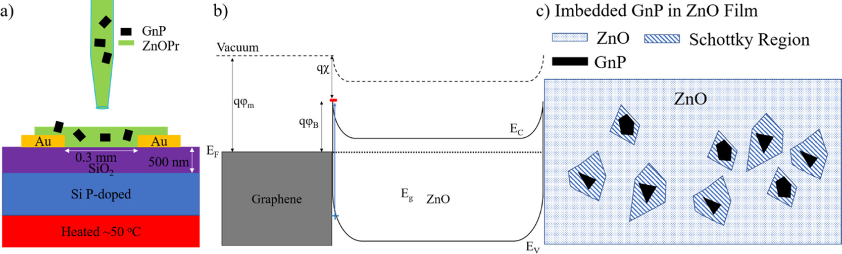
Figure 11: (a) Printing of ZnO precursor (ZnOPr)/graphene nanoplatelet composite ink, (b) energy band diagram of graphene and ZnO Schottky interface, and (c) a schematic of graphene nanoplatelets with the Schottky interface. 70 Copyright American Chemical Society, 2019. Reproduced with permission.
Lee et al reported ZnO ink in EtOH/EG solvent system. This ink system is suitable to form microporous networks of ZnO which absorbs more light than smooth ZnO films, which is useful for high performance photodetection 71. Microporosity results from different in evaporation rate of low boiling point solvent EtOH and high boiling point solvent EG. However, residual EG in the films can negatively impact the PD performance (Figure 12). To obtain the microporous films in the low boiling point cosolvent system EtOH/IPA, and to avoid high boiling pint EG solvent, Gr was introduced. ZnO and Gr layers were inkjet printed in a layer-by-layer fashion. Due to the surface tension difference between ZnO and Gr layer, microporous structures were formed. However, a lower concentration of Gr was required, as large concentrations will form conductive networks in ZnO which will increase the dark currents of PDs.

Figure 12: (a–c) Under 1 mW 405 nm irradiance, transient photocurrent plots of ZnO, layer-by-layer printed ZnO/G and annealed ZnO/G film for ZnO in EtOH/1-propanol (5:1) with graphene in EtOH (a), ZnO in EtOH/IPA (5:1) with Graphene in EtOH (b), and ZnO in EtOH/IPA (5:1) with graphene in DMF (c). (d–f) Height mapping for corresponding films: ZnO in EtOH/1-propanol (5:1) with graphene in EtOH (d), ZnO in EtOH/IPA (5:1) with graphene in EtOH (e), and ZnO in EtOH/IPA (5:1) with graphene in DMF (f). 71 Copyright American Chemical Society, 2020. Reproduced with permission.
Table 2: Performance of 2D materials based printed PDs
|
Printing method |
Structure |
Responsivity |
Detectivity |
Speed |
Light |
Ref. |
|
Inkjet printing |
MoS2/Gr (thermally annealed) |
∼1 mA/W |
∼4.31 × 10⁷ Jones |
0.15 ms |
515 nm |
|
|
Inkjet printing |
MoS2/Gr (Photonically annealed) |
∼50 mA/W |
3.18 × 10⁹ Jones |
5 ms |
550 nm |
|
|
Inkjet printing |
MoS2/Gr |
R ~ 0.11 A/W |
~ 1.7 × 10¹⁰ |
1.3 s |
|
|
|
Inkjet printing |
MoS2/Gr |
R ~ 0.3A/W |
|
|
|
|
|
Inkjet printing |
BP/Gr/Si |
196 mA/W at 450nm 1.8 mA/W at 1550 nm |
|
0.55 ms |
450, 1550 nm |
|
|
Inkjet printing |
WS2/Gr |
2.5 A/W |
|
|
532 nm |
|
|
Inkjet printing |
MoTe2/Gr |
120 mA/W @532 nm 7.7 mA/W at 940 nm |
|
|
532 nm, 940 nm |
|
|
Inkjet Printing |
MoS2/Gr |
6.5 µA @22 mW/cm2 |
|
|
|
|
|
Inkjet Printing |
β -InSe |
274 A/W |
|
15 ms |
455 |
|
|
Inkjet Printing |
ZnO/Gr |
7500 A/W |
|
0.18s |
365 nm |
|
|
Inkjet Printing |
ZnO/GnP |
2.2 A/W |
|
9.6 s |
340 nm |
|
|
Electro-hydrodynamic printing |
TMDC/Gr |
1.15 A/W |
|
|
|
|
|
Inkjet Printing |
WS2/Gr |
0.61 mA/W |
|
In seconds |
532 nm |
LPE is a viable method for the exfoliation of 2D materials for the development of the inks. Choice of 2D materials, properties of solvents (co-solvents, boiling point, surface tension, environmental factors), binder and stabilizer will define the final properties and printability of the inks. Choice of substrate is also very important, as not every ink can be printed smoothly on every substrate. Inks also need to be modified according to the printing technology. For example, Inkjet printing requires low or moderate viscosity, while screen printing needs high viscosity inks. Printing technology will also determine the resolution of the patterns. So far printed PDs have shown reasonably good performance, however, most of the printed PDs are either photoconductor or simple heterojunctions, as so far printing methods for fabrication of 2D heterojunctions have not matured yet. For future, focus should be on developing printing technologies for complex heterostructures of 2D materials with the inks. Also efforts should be focused on establishing structure-property relationship in 2D PDs as structure of 2D materials in inks is different from CVD grown or mechanically exfoliated materials. Moreover, residual binder, solvents and stabilizer also make it difficult to predict or control the PD performance.
This publication/paper has been produced benefiting from the 2232 International Fellowship for Outstanding Researchers Program of TÜBITAK (Project No: 118C214). However, the entire responsibility of the publication/paper belongs to the owner of the publication/paper. The financial support received from TÜBITAK does not mean that the content of the publication is approved in a scientific sense by TÜBITAK. Ayaz Ali acknowledges the grant from Higher Education Commission (HEC), Pakistan (Project No. 20-14470/NRPU/R&D/HEC/2021).
Bolton, Eric K, Sayler, Gary S, Nivens, David E, Rochelle, James M, Ripp, Steven & Simpson, Michael L . 2002. Integrated CMOS photodetectors and signal processing for very low-level chemical sensing with the bioluminescent bioreporter integrated circuit. Sensors and Actuators B: Chemical 85(1-2):179–185.
Rao, Gaofeng, Wang, Xuepeng, Wang, Yang, Wangyang, Peihua, Yan, Chaoyi, Chu, Junwei, Xue, Lanxin, Gong, Chuanhui, Huang, Jianwen, Xiong, Jie & Li, Yanrong . 2019. Two?dimensional heterostructure promoted infrared photodetection devices. InfoMat 1(3):272–288.
Yin, Chujun, Gong, Chuanhui, Chu, Junwei, Wang, Xudong, Yan, Chaoyi, Qian, Shifeng, Wang, Yang, Rao, Gaofeng, Wang, Hongbo, Liu, Yuqing, Wang, Xianfu, Wang, Jianlu, Hu, Weida, Li, Chaobo & Xiong, Jie . 2020. Ultrabroadband Photodetectors up to 10.6 µm Based on 2D Fe3O4 Nanosheets. Advanced Materials 32(25):2002237.
Wang, Xiaomu, Cheng, Zhenzhou, Xu, Ke, Tsang, Hon Ki & Xu, Jian-Bin . 2013. High-responsivity graphene/silicon-heterostructure waveguide photodetectors. Nature Photonics 7(11):888–891.
Shehzad, Khurram, Shi, Tianjin, Qadir, Akeel, Wan, Xia, Guo, Hongwei, Ali, Ayaz, Xuan, Weipeng, Xu, Hua, Gu, Zhongze, Peng, Xinsheng, Xie, Jin, Sun, Litao, He, Qiyuan, Xu, Zhen, Gao, Chao, Rim, You-Seung, Dan, Yaping, Hasan, Tawfique, Tan, Pingheng, Li, Erping, Yin, Wenyan, Cheng, Zhiyuan, Yu, Bin, Xu, Yang, Luo, Jikui & Duan, Xiangfeng . 2017. Designing an Efficient Multimode Environmental Sensor Based on Graphene-Silicon Heterojunction. Advanced Materials Technologies 2(4):1600262.
Casalino, M, Coppola, G, Iodice, M, Rendina, I & Sirleto, L . 2012. Near-Infrared All-Silicon Photodetectors. International Journal of Photoenergy 2012:1–6.
Huang, Zhihong, Carey, James E, Liu, Mingguo, Guo, Xiangyi, Mazur, Eric & Campbell, Joe C . 2006. Microstructured silicon photodetector. Applied Physics Letters 89(3):033506.
Downs, C & Vandervelde, T E . 2000. Progress in infrared photodetectors since 13:5054–98.
Jagadish, C, Gunapala, S & Rhiger, D . 2011. Advances in infrared photodetectors. Elsevier
Bolotin, K I, Sikes, K J, Jiang, Z, Klima, M, Fudenberg, G, Hone, J, Kim, P & Stormer, H L . 2008. Ultrahigh electron mobility in suspended graphene. Solid State Communications 146(9-10):351–355.
Schedin, F, Geim, A K, Morozov, S V, Hill, E W, Blake, P, Katsnelson, M I & Novoselov, K S . 2007. Detection of individual gas molecules adsorbed on graphene. Nature Materials 6(9):652–655.
Dong, Tao, Simões, João & Yang, Zhaochu . 2020. Flexible Photodetector Based on 2D Materials: Processing, Architectures, and Applications. Advanced Materials Interfaces 7(4):1901657.
Huo, Nengjie & Konstantatos, Gerasimos . 2018. Recent Progress and Future Prospects of 2D-Based Photodetectors. Advanced Materials 30(51):1801164.
Du, S, Lu, W, Ali, A, Zhao, P, Shehzad, K & Guo, H . 2017. A broadband fluorographene photodetector 29:1700463.
Xu, Yang, Ali, Ayaz, Shehzad, Khurram, Meng, Nan, Xu, Mingsheng, Zhang, Yuhan, Wang, Xinran, Jin, Chuanhong, Wang, Hongtao, Guo, Yuzheng, Yang, Zongyin, Yu, Bin, Liu, Yuan, He, Qiyuan, Duan, Xiangfeng, Wang, Xiaomu, Tan, Ping?heng, Hu, Weida, Lu, Hai & Hasan, Tawfique . 2017. Solvent?Based Soft?Patterning of Graphene Lateral Heterostructures for Broadband High?Speed Metal–Semiconductor–Metal Photodetectors. Advanced Materials Technologies 2(2):1600241.
Chen, X, Shehzad, K, Gao, L, Long, M, Guo, H & Qin, S . 2020. Graphene hybrid structures for integrated and flexible optoelectronics 32:1902039.
Yao, J & Yang, G . 2020. 2D material broadband photodetectors. Nanoscale 12:454–76.
Torrisi, Felice & Coleman, Jonathan N . 2014. Electrifying inks with 2D materials. Nature Nanotechnology 9(10):738–739.
Moses, O A, Gao, L, Zhao, H, Wang, Z, Adam, M L & Sun, Z . 2021. 2D materials inks toward smart flexible electronics 50:116–164.
Hu, Guohua, Kang, Joohoon, Ng, Leonard W T, Zhu, Xiaoxi, Howe, Richard C T, Jones, Christopher G, Hersam, Mark C & Hasan, Tawfique . 2018. Functional inks and printing of two-dimensional materials. Chemical Society Reviews 47(9):3265–3300.
Huo, C, Yan, Z, Song, X & Zeng, H . 2015. 2D materials via liquid exfoliation: a review on fabrication and applications 60:1994–2008.
Mcmanus, Daryl, Vranic, Sandra, Withers, Freddie, Sanchez-Romaguera, Veronica, Macucci, Massimo, Yang, Huafeng, Sorrentino, Roberto, Parvez, Khaled, Son, Seok-Kyun, Iannaccone, Giuseppe, Kostarelos, Kostas, Fiori, Gianluca & Casiraghi, Cinzia . 2017. Water-based and biocompatible 2D crystal inks for all-inkjet-printed heterostructures. Nature Nanotechnology 12(4):343–350.
Ricciardulli, Antonio Gaetano & Blom, Paul W M . 2020. Solution?Processable 2D Materials Applied in Light?Emitting Diodes and Solar Cells. Advanced Materials Technologies 5(8):1900972.
Brennen, C E . 2014. Cavitation and bubble dynamics. Cambridge university press
Chen, Xianjue, Dobson, John F & Raston, Colin L . 2012. Vortex fluidic exfoliation of graphite and boron nitride. Chemical Communications 48(31):3703.
Paton, Keith R, Varrla, Eswaraiah, Backes, Claudia, Smith, Ronan J, Khan, Umar, O’neill, Arlene, Boland, Conor, Lotya, Mustafa, Istrate, Oana M, King, Paul, Higgins, Tom, Barwich, Sebastian, May, Peter, Puczkarski, Pawel, Ahmed, Iftikhar, Moebius, Matthias, Pettersson, Henrik, Long, Edmund, Coelho, João, O’brien, Sean E, Mcguire, Eva K, Sanchez, Beatriz Mendoza, Duesberg, Georg S, Mcevoy, Niall, Pennycook, Timothy J, Downing, Clive, Crossley, Alison, Nicolosi, Valeria & Coleman, Jonathan N . 2014. Scalable production of large quantities of defect-free few-layer graphene by shear exfoliation in liquids. Nature Materials 13(6):624–630.
Frindt, R & Yoffe, A . 1963. Physical properties of layer structures: optical properties and photoconductivity of thin crystals of molybdenum disulphide. Proceedings of the Royal Society of London Series A Mathematical and Physical Sciences 273:69–83.
Ma, R & Sasaki, T . 2010. Nanosheets of Oxides and Hydroxides: Ultimate 2D Charge-Bearing Functional Crystallites 22:5082–104.
Eda, G, Yamaguchi, H, Voiry, D, Fujita, T, Chen, M & Chhowalla, M . 2011. Photoluminescence from chemically exfoliated MoS2 11:5111–5117.
Witomska, Samanta, Leydecker, Tim, Ciesielski, Artur & Samorì, Paolo . 2019. Production and Patterning of Liquid Phase–Exfoliated 2D Sheets for Applications in Optoelectronics. Advanced Functional Materials29(22):1901126.
Yang, Yingchang, Hou, Hongshuai, Zou, Guoqiang, Shi, Wei, Shuai, Honglei, Li, Jiayang & Ji, Xiaobo . 2019. Electrochemical exfoliation of graphene-like two-dimensional nanomaterials. Nanoscale 11(1):16–33.
Donato, M G, Vasi, S, Sayed, R, Jones, P H, Bonaccorso, F, Ferrari, A C, Gucciardi, P G & Maragò, O M . 2012. Optical trapping of nanotubes with cylindrical vector beams. Optics Letters 37(16):3381.
Howe, Richard C T, Woodward, Robert I, Hu, Guohua, Yang, Zongyin, Kelleher, Edmund J R & Hasan, Tawfique . 2016. Surfactant-aided exfoliation of molybdenum disulfide for ultrafast pulse generation through edge-state saturable absorption. physica status solidi (b) 253(5):911–917.
Hasan, T, Torrisi, F, Sun, Z, Popa, D, Nicolosi, V, Privitera, G, Bonaccorso, F & Ferrari, A C . 2010. Solution-phase exfoliation of graphite for ultrafast photonics. physica status solidi (b) 247(11-12):2953–2957.
Green, Alexander A & Hersam, Mark C . 2009. Solution Phase Production of Graphene with Controlled Thickness via Density Differentiation. Nano Letters 9(12):4031–4036.
Guardia, L, Fernández-Merino, M J, Paredes, J I, Solís-Fernández, P, Villar-Rodil, S, Martínez-Alonso, A & Tascón, J M D . 2011. High-throughput production of pristine graphene in an aqueous dispersion assisted by non-ionic surfactants. Carbon 49(5):1653–1662.
Hasan, T, Sun, Z, Wang, F, Bonaccorso, F, Tan, P H & Rozhin, A G . 2009. Nanotube-Polymer Composites for Ultrafast Photonics 21:3874–99.
Kim, F, Cote, L J & Huang, J . 2010. Graphene oxide: surface activity and two?dimensional assembly. Advanced Materials 22(17):1954–1962.
Lee, Stephanie S, Kim, Chang Su, Gomez, Enrique D, Purushothaman, Balaji, Toney, Michael F, Wang, Cheng, Hexemer, Alexander, Anthony, John. E & Loo, Yueh-Lin . 2009. Controlling Nucleation and Crystallization in Solution-Processed Organic Semiconductors for Thin-Film Transistors. Advanced Materials 21(35):3605–3609.
Chen, Jihua, Tee, Chee Keong, Shtein, Max, Martin, David C & Anthony, John . 2009. Controlled solution deposition and systematic study of charge-transport anisotropy in single crystal and single-crystal textured TIPS pentacene thin films. Organic Electronics 10(4):696–703.
Wang, S, Kappl, M, Liebewirth, I, Mtin, M & Anthony, J . 2012. Controlled solution deposition and systematic study of charge-transport anisotropy gle polymer fibers. Advanced materials 417–437.
Saidina, D S, Zubir, S A, Fontana, S, Hérold, C & Mariatti, M . 2019. Synthesis and Characterization of Graphene-Based Inks for Spray-Coating Applications. Journal of Electronic Materials 48(9):5757–5770.
Garakani, Mohammad Akbari, Bellani, Sebastiano, Pellegrini, Vittorio, Oropesa-Nuñez, Reinier, Castillo, Antonio Esau Del Rio, Abouali, Sara, Najafi, Leyla, Martín-García, Beatriz, Ansaldo, Alberto, Bondavalli, Paolo, Demirci, Cansunur, Romano, Valentino, Mantero, Elisa, Marasco, Luigi, Prato, Mirko, Bracciale, Gaetan & Bonaccorso, Francesco . 2021. Scalable spray-coated graphene-based electrodes for high-power electrochemical double-layer capacitors operating over a wide range of temperature. Energy Storage Materials 34:1–11.
Norrman, K, Ghanbari-Siahkali, A & Larsen, N B . 2005. 6 Studies of spin-coated polymer films. Annual Reports Section "C" (Physical Chemistry) 101:174.
Akuzum, Bilen, Maleski, Kathleen, Anasori, Babak, Lelyukh, Pavel, Alvarez, Nicolas Javier, Kumbur, E Caglan & Gogotsi, Yury . 2018. Rheological Characteristics of 2D Titanium Carbide (MXene) Dispersions: A Guide for Processing MXenes. ACS Nano 12(3):2685–2694.
Leach, R . 2012. The printing ink manual. Springer Science & Business Media
Kang, Boseok, Lee, Wi Hyoung & Cho, Kilwon . 2013. Recent Advances in Organic Transistor Printing Processes. ACS Applied Materials & Interfaces 5(7):2302–2315.
Zhang, D W, Li, X D, Li, H B, Chen, S, Sun, Z, Yin, X J & Huang, S M . 2011. Graphene-based counter electrode for dye-sensitized solar cells. Carbon 49(15):5382–5388.
Xu, Chaohe, Xu, Binghui, Gu, Yi, Xiong, Zhigang, Sun, Jing & Zhao, X S . 2013. Graphene-based electrodes for electrochemical energy storage. Energy & Environmental Science 6(5):1388.
Hyun, Woo Jin, Secor, Ethan B, Hersam, Mark C, Frisbie, C Daniel & Francis, Lorraine F . 2015. High-Resolution Patterning of Graphene by Screen Printing with a Silicon Stencil for Highly Flexible Printed Electronics. Advanced Materials 27(1):109–115.
Hutchings, I M & Martin, G D . 2013. Inkjet technology for digital fabrication. Online Library: Wiley
An, B W, Kim, K, Lee, H, Kim, S Y, Shim, Y & Lee, D Y . 2015. Hightion: Wiley Online g of 3D structures using an electrohydrodynamic inkjet with multiple functional inks. Advanced materials 27:4322–4330.
Song, Donghoon, Mahajan, Ankit, Secor, Ethan B, Hersam, Mark C, Francis, Lorraine F & Frisbie, C Daniel . 2017. High-Resolution Transfer Printing of Graphene Lines for Fully Printed, Flexible Electronics. ACS Nano 11(7):7431–7439.
Jang, Daehwan, Kim, Dongjo & Moon, Jooho . 2009. Influence of Fluid Physical Properties on Ink-Jet Printability. Langmuir 25(5):2629–2635.
Hu, Guohua, Albrow-Owen, Tom, Jin, Xinxin, Ali, Ayaz, Hu, Yuwei, Howe, Richard C T, Shehzad, Khurram, Yang, Zongyin, Zhu, Xuekun, Woodward, Robert I, Wu, Tien-Chun, Jussila, Henri, Wu, Jiang-Bin, Peng, Peng, Tan, Ping-Heng, Sun, Zhipei, Kelleher, Edmund J R, Zhang, Meng, Xu, Yang & Hasan, Tawfique . 2017. Black phosphorus ink formulation for inkjet printing of optoelectronics and photonics. Nature Communications 8(1):1–10.
Secor, E B, Prabhumirashi, P L, Puntambekar, K, Geier, M L & Hersam, M C . 2013. The journal of physical chemistry letters 4:1347–51.
Goldschmidt, A & Streitberger, H.-J . 2003. BASF handbook on basics of coating technology: William Andrew.
Lahti, M, Leppävuori, S & Lantto, V . 1999. Gravure-offset-printing technique for the fabrication of solid films. Applied Surface Science 142(1-4):367–370.
Bonaccorso, F, Bartolotta, A, Coleman, J N & Backes, C . 2016. 2D?crystal?based functional inks. Advanced Materials 28(29):6136–6166.
Lahti, M, Leppävuori, S & Lantto, V . 1999. Gravure-offset-printing technique for the fabrication of solid films. Applied Surface Science 142(1-4):367–370.
Seo, Jung-Woo Ted T, Zhu, Jian, Sangwan, Vinod K, Secor, Ethan B, Wallace, Shay G & Hersam, Mark C . 2019. Fully Inkjet-Printed, Mechanically Flexible MoS2 Nanosheet Photodetectors. ACS Applied Materials & Interfaces 11(6):5675–5681.
Hossain, Ridwan Fayaz, Bandyopadhyay, Avra S & Kaul, Anupama B . 2022. Vibrational spectroscopy on solution-dispersed MoS2 for inkjet-printed photodetectors. Emergent Materials 5(2):477–487.
Hossain, Ridwan F, Min, Misook & Kaul, Anupama B . 2019. High-Performance, Flexible, Inkjet Printed Heterostructure Photodetector for Biosensing Applications. MRS Advances 4(10):621–627.
Hossain, Ridwan F, Deaguero, Isaac G, Boland, Thomas & Kaul, Anupama B . 2016. Solution dispersed 2D graphene & MoS2 for an inkjet printed biocompatible photodetector. 2016 Lester Eastman Conference (LEC) 19–22.
Abate, Yohannes, Akinwande, Deji, Gamage, Sampath, Wang, Han, Snure, Michael, Poudel, Nirakar & Cronin, Stephen B . 2018. Recent Progress on Stability and Passivation of Black Phosphorus. Advanced Materials 30(29):1704749.
Wan, Xi, Gao, Mingliang, Xu, Shijia, Huang, Tianhao, Duan, Yaoyu, Chen, Enzi, Chen, Kun, Zeng, Xiaoliang, Xie, Weiguang & Gu, Xiaofeng . 2022. Inkjet-printed TMDC–graphene heterostructures for flexible and broadband photodetectors. Journal of Applied Physics 131(23):234303.
Curreli, Nicola, Serri, Michele, Spirito, Davide, Lago, Emanuele, Petroni, Elisa, Martín?garcía, Beatriz, Politano, Antonio, Gürbulak, Bekir, Duman, Songül, Krahne, Roman, Pellegrini, Vittorio & Bonaccorso, Francesco . 2020. Liquid Phase Exfoliated Indium Selenide Based Highly Sensitive Photodetectors. Advanced Functional Materials 30(13):1908427.
Alzakia, Fuad Indra, Tang, Baoshan, Pennycook, Stephen John & Tan, Swee Ching . 2020. Engineering the photoresponse of liquid-exfoliated 2D materials by size selection and controlled mixing for an ultrasensitive and ultraresponsive photodetector. Materials Horizons 7(12):3325–3338.
Leng, T, Parvez, K, Pan, K, Ali, J, Mcmanus, D & Novoselov, K S . 2020. Printed graphene/WS2 battery-free wireless photosensor on papers. 2D Materials 7(2):24004.
Cook, Brent, Gong, Maogang, Corbin, Alex, Ewing, Dan, Tramble, Ashley & Wu, Judy . 2019. Inkjet-Printed Imbedded Graphene Nanoplatelet/Zinc Oxide Bulk Heterojunctions Nanocomposite Films for Ultraviolet Photodetection. ACS Omega 4(27):22497–22503.
Lee, Hanleem, Harden-Chaters, William, Han, Soo Deok, Zhan, Shijie, Li, Benxuan, Bang, Sang Yun, Choi, Hyung Woo, Lee, Sanghyo, Hou, Bo, Occhipinti, Luigi G & Kim, Jong Min . 2020. Nano-to-Microporous Networks via Inkjet Printing of ZnO Nanoparticles/Graphene Hybrid for Ultraviolet Photodetectors. ACS Applied Nano Materials 3(5):4454–4464.
Keywords: 2D materials. Photodetectors, Printed, Inks
Materials Innovations (MI) is an interdisciplinary journal devoted to significant experimental and theoretical findings on the synthesis, structure, charachterization, processing and applications of materials. Materials Innovations is dedicated to publishing peer reviewed novel, cutting edge reports of broad interest to the materials science community.