Materials Innovations
Full Html
Vol 1 Issue 1
Insight into the Opto-electronic Properties of AgGas2 under Axial Strain via ab-initio Calculations
Pages: 34-45
Doi:
Doi URL: http://doi.org/10.54738/MI.2021.1101
Nazia Erum 1 , Muhammad Azhar Iqbal 2 , Sadia Sagar 1 , Muhammad Nawaz 1
1 Physics Department, The University of Lahore, New Campus, Lahore, Pakistan
2 Department of Physics, University of the Punjab, QuaidAzam Campus, Lahore, Pakistan
The density functional theory technique based on the Full Potential Linear Augmented Plane Wave (FP-LAPW) method is used to investigate the structural, electronic, and optical properties of AgGaS 2 under different values of axial strain. The structural parameters are in good accordance with experimental ones. Furthermore, the Tran-Blaha modi?ed Becke-Johnson (TB-mBJ) potential method is used to achieve the desired band structure, which verifies the experimental results. It is observed that when tensile strain (0%, +3%, +6%, +9%) is applied, the bandgap reduces from 2.253 eV to 1.645 eV and when compressive strain (0%, -3%, -6%, - 9%) is applied, band gap increases from 2.253 eV to 2.9331 eV. Axial strain enhances the absorption, reflection and refractive index, which compromises the transparent performance in visible region. Due to high absorption coefficient and close to the optimal bandgap, AgGaS 2 is a suitable material for solar cell and light emitting diodes and related applications. The main focus of the study is to tune bandgap and optical properties of AgGaS 2 by using biaxial tension.
Keywords
AgGaS2, Electrical properties, Optical properties, Strain
Chalcopyrite semiconductor have been extensively used in numerous applications like solar cells, photo-detectors, flat panel displays, gas sensors and Laser diodes.1,2 These materials have direct band gap of about (~2 eV), which makes them transparent for visible light. Using biaxial practices, strain has been used to tune the band gap of these materials for various applications. Several researchers have been working on AI III CVI family exploring linear and non-optical properties. Few works have reported the structural, elastic and optical properties of these semiconductors by using Density Functional Theory (DFT). Several researchers focused on reporting the theoretical analysis of the AgGaX2 (X = S, Se, Te) chalcopyrites. The equation (ZT= S2rT/k) shows that greater the ZT, there will be more effective energy conversion and eventually minor the thermal conductivity due to its inverse relation with each other.1,2 Kurosaki and coworkers reported that AgGaS2 compound has minor thermal conductivity at room temperature so k value will be lower with the rise in temperature and vice versa.3In 2019, Omamoke and Enaroseha calculated the electronic and optical properties of AgGaS2 and AgGaSe2 by utilizing pseudopotential method Projector Augmented Wave method (PAW). This?technique, gives results which match closely with the experimental findings. Computational findings show that both materials are semiconductors and have band gap 1.82 eV and 1.25 eV respectively. The density of states and partial density of states showed that Ga-4s orbital has greater energy than the Ga-3p orbital.4 In 2017, Hou et al. investigated the ground state parameters such as lattice constants, bulk modulus and elastic constants for AgAlS2chalcopyrite structure by using Den- sity Functional Theory (DFT). The obtained lattice parameters and elastic constants agreed well with available theoretical and experimental results. The bulk modulus B, shear modulus G, Young’s modulus E and wave velocity of AgAlS2 were also obtained for the first time. In addition, the equation of state of AgAlS2 in the pressure range of 0-10 GPa and up to temperature of 1000 K was stated.5
H. Salehi, E. Gordanian et al. deter- mined structural, electronic and optical characteristics of AgGaX2 (X=Te, S, Se) with the help of Engel Vosco Gen- eralized Gradient Approximation (EV-GGA). For optical and band gap characteristics, mBJ was in good favor with experimental and our calculated results. Furthermore, lattice constant and bulk modulus (B) GGA-PBE results were close to experimental work. Band configuration, which was straight for all components were plotted to achieve band gap and other electronic characteristics such as total and partial Density of States. The function of X atoms (X = Te, S, Se) in optical properties such as extinction coefficient, reflection coefficient, and refractive index, using imaginary and real sections of dielectrics were also investigated.6
Yi Li, and his fellows proposed a specialized genetic algorithm approach in combination with first-principles calculations to predict the stable structures of AgGaS2 crystal at different pressures. The results show that the chalcopyrite structure first transforms to the monoclinic phase, and then to a centrosymmetric structure due to which second-harmonic generation (SHG) response of AgGaS2 disappears. The effects of external pressures, up to 7 GPa, on the linear and second- order nonlinear optical properties of AgGaS2 are explored systematically. This work reveals that the resistance to laser-induced damage, the transparency range, and the phase matchability can be improved by the pressure-induced deformation of AgGaS2 crystal. Moreover, the feature of the strong SHG response of AgGaS2 crystal is still preserved in the whole IR region even under pressure up to 7 GPa.7
AgGaS2 have attained the attention in opto-electronics and non-linear optical properties due to their potential use. Some of the application such as light emitting diodes (LED), solar cells, photovoltaic detectors, optical frequency conversion, laser frequency conversion, and signal communications, etc.5,6 Due to unique electronic configurations of this compound, d-shell elections participate in conduction process which can be used to enhance the effectiveness of electrical and optical properties. The main objective of our studies is to calculate the lattice parameters of AgGaS2 under axial strain, to study (under strain) detailed opto-electronic properties including total and partial Density of states, band structure, absorption coefficient, refractive index, extinction coefficient, and reflectivity. Detailed results of our study are presented below, which can be useful for the various electronic and opto-electronic applications of AgGaS2. We believe that our results on strain induced changes in electrical and optical properties of AgGaS2 will be useful for scientist working in experimental and computational Materials Science.
To calculate under axial strain structural and opto-electronic properties of AgGaS2, the Full Potential Linearized Augmented Plane Wave (FP-LAPW) method is applied to elucidate Khon- Sham equations7 derived in DFT, by means of different exchange correlation approximations like GGA-PBE, GGA-PBE-sol and GGA plus Trans-Blaha modified Becke–Johnson (TB- mBJ) potential.8 Additionally, optimizations of each unit cell are per- formed to obtain ground state structural parameters by fitting Birch-Murnaghan equation of state.9 Moreover, In WIEN2K package, valence electrons treatment is done semi-relativistically although, core electrons are treated fully relativistically.11 But for convergence in basis size a cut-off value of R MT K max = 8.0 is used. Additionally, to achieve well-converged optimum results of structural properties, 56 K point integration in brillouin zone (BZ) is done with modified form of tetrahedron method. Furthermore, for calculating opto-electronic, properties a denser mesh of 2000 K-points is used. The converged calculations are achieved, when the energy difference between two consecutive self-consistent cycles was seems to be less than 0.01 mRy and 0.1m for energy and charge, respectively.
At room temperature and pressure, the AgGaS2 unit cell is in the tetragonal phase with space group. I_42d (No .122). Its unit cell consists of three molecules, each of which has an Ag atom at position (0, 0, 1/2): (0, 1/2, 3/4), Ga at (0, 0, 0), (0, 1/2, 1/4) and S2 at (u, 1/4, 5/8), (1/4, u, 2/5), (u, 3/4, 7/8), (3/4, u, 2/5). Where the value of u = 0.26 (common structural position) as shown in Figure 1. We measure the energy as a volume function to reduce the total energy of said compound in accordance with other geometrical parameters as shown in Figure 2(a & b). In order to calculate structural properties of AgGaS2, the energy minimization process is employed, where the total energy (E) and the corresponding equilibrium cell volume (V o ) are calculated by taking series of different lattice parameters. For each volume, the c/a quantity is determined, and a polynomial is then tuned to resolute energies in order to determine the best c/a proportion. As a result, an optimal bend (c/a) appears as a volume part.

Figure 1: Tetragonal structure of AgGaS2.
The obtained structural properties of AgGaS2 with tensile and compressive strain are listed in Table 1. The experimental lattice parameters of AgGaS2 structure are a = b = 5.756A ? c = 10.301 A0 and c/a = 1.7896A0. AgGaS2 is tetragonal. So, both a and b parameters are equivalent while c is not equivalent, and it is different from a and b.
Table 1: Structural properties of AgGaS2 with tensile and compressive strain.a Ref.12. b Ref.13 (other theoretical Work).c Ref.14 (experimental work).
|
Properties of the material and the structure |
Current work |
Other work |
Experimental work |
|
AgGaS2 a(Å) c(Å) c/a |
5.7875 10.6086 1.8327 |
5.756a/5.858 b 10.30a /10.39b 1.789 a /1.952b |
5.756c 10.34c 1.789c |
|
AgGaS2 for 3% strain a(Å) c(Å) c/a |
5.9891 10.6488 1.7780 |
--- |
--- |
|
AgGaS2 for 6% strain a(Å) c(Å) c/a |
6.1635 10.6488 1.7277 |
--- |
--- |
|
AgGaS2 for 9% strain a(Å) c(Å) c/a |
6.3379 10.6488 1.6802 |
--- |
--- |
|
AgGaS2 for -3% strain a(Å) c(Å) c/a |
5.64021 10.6488 1.8880 |
--- |
--- |
|
AgGaS2 for -6% strain a(Å c(Å) c/a |
5.46577 10.6488 1.9483 |
--- |
--- |
|
AgGaS2 for -9% strain a(Å) c(Å) c/a |
5.29133 10.6488 2.0125 |
--- |
--- |
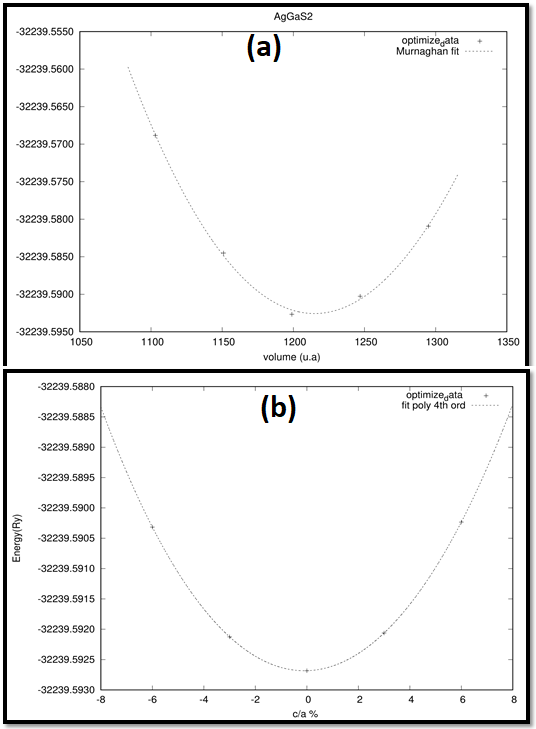
Figure 2: Volume optimization of AgGaS2 with (a) PBE-GGA (Murnaghan fit) (b) PBE-GGA (fit poly 4th order).
To examine the effect of the compressive strain on the electronic properties in AgGaS2 compound, we first determine properties of AgGaS2. The electronic characteristics are determined by using Trans Blaha modified Becke Johnson potential (TB-mBJ) potential. The electronic band structure and Density of states (DOS) for 0% strain with TB-mBJ potential are presented in Figure 3(a) and Figure 3(b), respectively. The plot is energy against high symmetry points in the first Brillioun zone. The valence and conduction band’s energies are grouped together. The Fermi energy, which is represented by dotted lines, is set at zero energy. The minima and maxima of the conduction and valence bands remain unchanged. It indicates that CBM and VBM are at a negative value, indicating that AgGaS2 possess direct band gap. The fundamental band gap is direct and occurs at the gamma point, which means that the conduction band minimum (CBM) and the valence band maximum (VBM) are both on the gamma point. The band gap of AgGaS2 is 2.25 eV. The calculated results for bandgap are in reasonable agreement with experimental values of 2.14 eV15 and 2.23 eV.16,17 Furthermore, the orbital contribution from Ag to the total density of states are the 4s, 4p, 4d and 5s orbitals. The orbital contribution from Ga is 3d states, p orbital contribution is from the 3p and 4p and 4s orbital. The orbital contribution from S is S-3p, S- 3s, orbital, respectively. It is observed that valence band in energy region from 5eV to 0eV dominated states are Ag- 4d, Ga-4p and S-3p states. At energy level from -10 eV to -5 eV Ga-4p states are dominated and in -5 eV to -0 eV energy region dominated states are S2-3s while energy region -10 eV to -5 eV is subsidized by Ga-4p state. The low- est part of the conduction band, from 0 to 5 eV energy range Ga-4s, Ga- 4p, and S-3p states are more valuable, while in the energy range from 5 eV to 15 eV, the Ga-4s, Ga-4p, and S-3p states are more valuable. Ga-4p and S-3p, Ga-3d, S-3p, and S-3s are all strong contributors.
The electronic band structure for 0 %, 3 %, 6 %, 9 %, and -3 %, -6 %, -9 % strain with TB-mBJ potential are presented in Figure 4. It can be noticed that as strain start to increase from 0 to 9 % the fundamental band gap remains direct and occurs at the gamma point, which means that the conduction band minimum (CBM) and the valence band maximum (VBM) are both on the gamma point but the bandgap going to decrease from 2.253 eV to 1.645 eV. On the other hand, as strain start to decrease from 0 to -9 % the fundamental band gap remains still direct and occurs at the gamma point, but bandgap increase from 2.253 eV to 2.933 eV as shown in Table 1.
The total and partial density of states (TDOS & PDOS) for 0 percent, 3 %, 6 %, 9 %, and -3 %, -6 %, -9 % strain with TB-mBJ potential are presented in Figure 5 and Figure 6 respectively. Similar behavior of contraction and extraction is observed for TDOS & PDOS as noticed from bands dispersion curves. Compressed valence band is frequently contributed due to Ag-4d, Ga-4s and S-3p states from energy region -5 eV to 0 eV and with increased strain contribution, Ga-4p become more dominated. In forward direction, from energy level -10 eV to -5 eV Ga-4p and S2 -3p states more dominated but with cumulative strain the contribution of these situations is additional. It is further noticed that valence band from energy region -5 eV to -0 eV is dominated by S2-3s state however in energy region from -10 eV to -5eV dominated states are Ga-4p. It is observed that with further growing strain more hybridization states are produced. For the lowest part of conduction band from energy region 0 eV to 5 eV, more contribution is observed from Ga-4s, Ga-4p and S-3p states whereas in upper part from energy region 5 eV to 15 eV, more contribution is observed from Ga-4p and S-3p states while Ga-3d, S-3p and S-4d states are strongly hybridized. With additional collective strain Ga-3d, S-3p and S-4d become even more strongly hybridized. In case of total density of states, lowest part of conduction band from energy region 0 eV to 5 eV Ga-4p, and S-3s is dominated but from energy region from +10 eV to 15 eV Ga-4p and S-4d contributes more and strongly hybridized. It is observed that with the tensile strain edge of conduction band moves away from the Fermi-level.
Partial density of states (DOS), (Figure 6) are frequently governed by Ag-4d, Ga-4p and S-3p states from energy region -5 eV to 0 eV. In forward direction from energy level -10 eV to -5 eV Ga-4p and S2-3p states are strongly hybridized. It is observed that valence band from energy region -5 eV to 0 eV is influenced by S2-3s state while in forward direction energy region -10 eV to -5 eV is more contributed by Ga-4p state. It is possible that as strain decreases from -5 eV to 0 eV, Ga-5p state contribution decreases, while S-3s state contribution increases from -15 eV to -5 eV. From 0 eV to 5 eV, the lowest portion of the conduction band Ga-4s, Ga-4p, and S-3p states are more prominent and Ga-3d, S-3p, and S-4d are heavily hybridized in the upper part (energy range from 5 eV to 15 eV). It is noted that with decreasing strain from energy region 0 eV to 5 eV the contribution of S-3p is decreased but Ga-4s state is enhanced. The feedback of Ga-3d and 4p states increases in the forward direction from 5 eV to 15 eV, but the output of S-3p and 3s states decreases. In the case for total density of states, the lowest portion of the conduction band, (energy region 0 eV to 5 eV) contribution of S-3s and Ga-4p is dominant. As a result, the compressive strain is increased and the contribution of conduction band dominates near the Fermi-level.
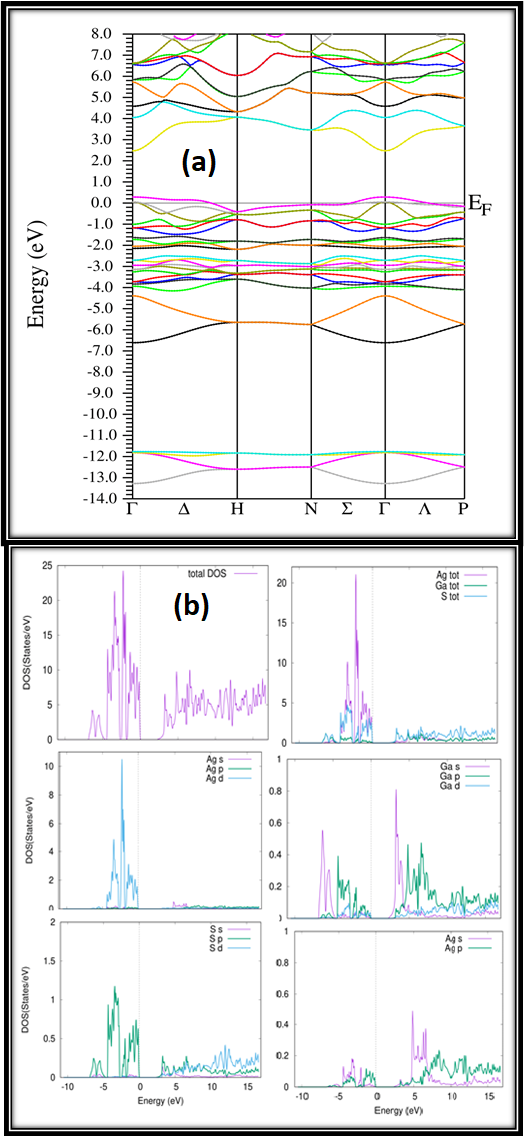
Figure 3: Calculated (a) band structure (b) total and partial density of states.
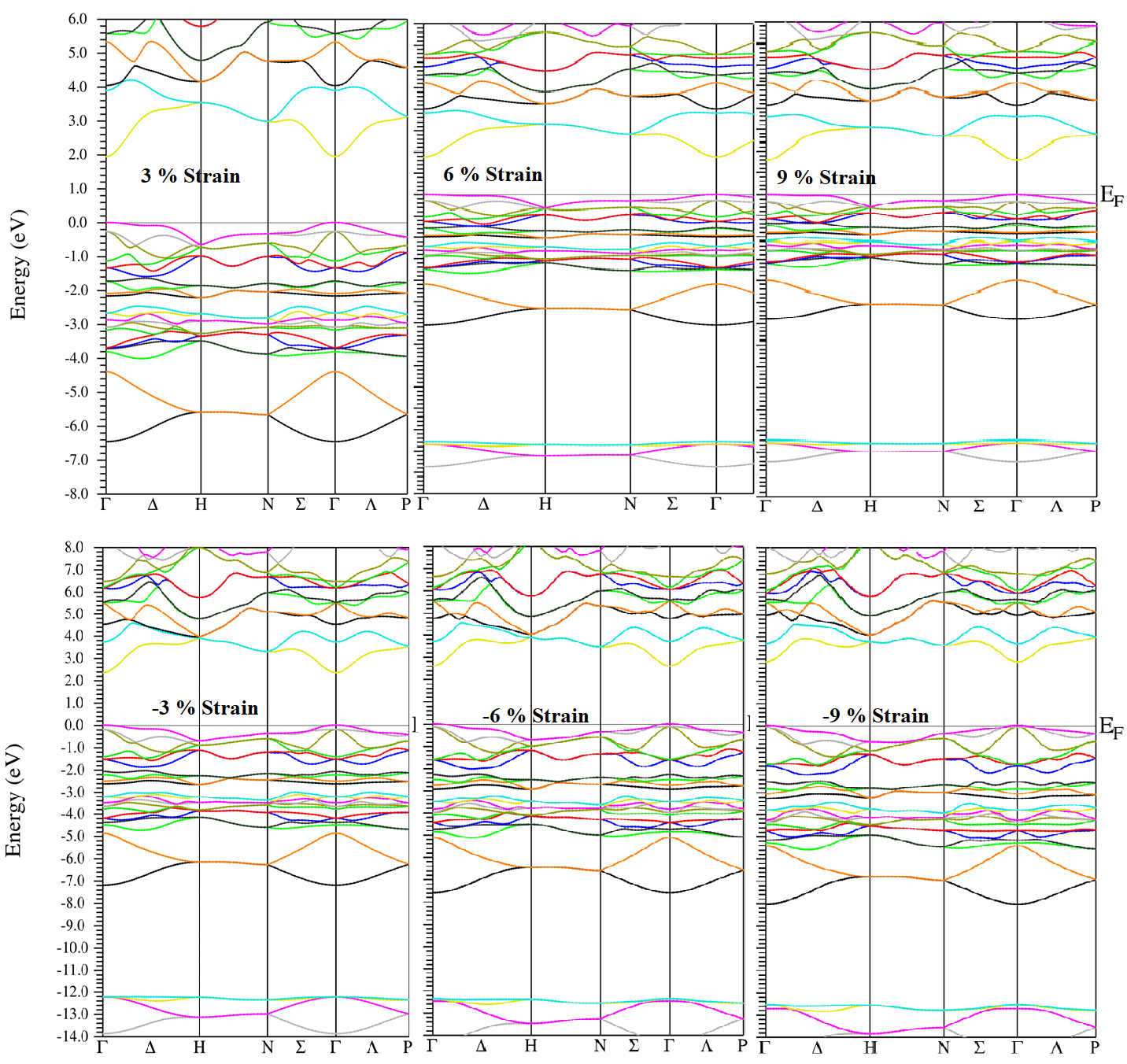
Figure 4: Calculated band structure of AgGaS2 for 3%, 6%, 9%, -3%, -6%, -9% strain with TB-mBJ
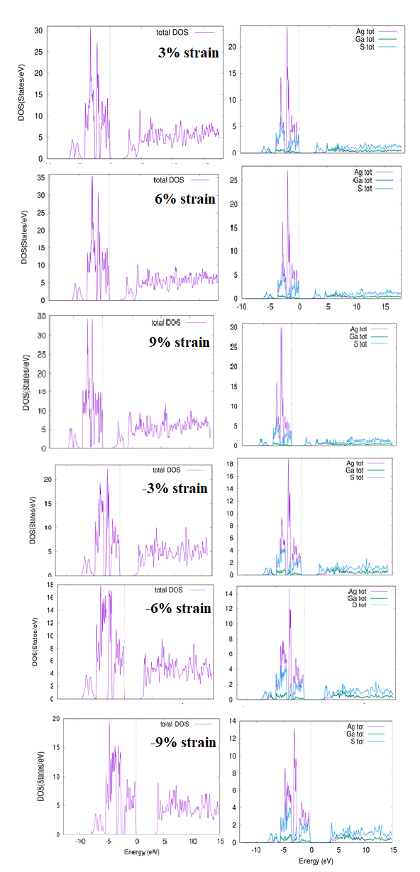
Figure 5: Calculated total density of states AgGaS2 for 3%, 6%, 9%,- 3%, -6%, -9% strain with TB-mBJ.
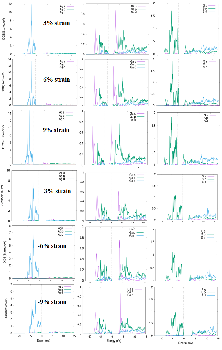
Figure 6: Calculated total density of states AgGaS2 for 3%, 6%, 9%, -3%, -6%, -9% strain with TB-mBJ.
Table 2: Calculated band gap of AgGaS2 for tensile and compressive strain.
|
Material AgGaTe2 |
Present work (TB-mBJ) |
|
-9% -6% -3% 0% 3% 6% 9% |
2.933 eV, 2.660 eV, 2.420 eV, 2.253eV, 1.999 eV, 1.831 eV, 1.645 eV |
The change in optical properties will give us further insight into the effects of strain on AgGaS2 electronic structure.18, 19 The optical properties of strained AgGaS2 are vital for opto-electronic devices and photovoltaic function. Calculated refractive index for 0%, 3%, 6%, 9% strain along x-axis and z-axis are shown in Figure 7 (a) & (b). The speed of light propagation fluctuates with tensile strain which shows high interference between incident light and medium.20–22 The refractive index value of tensile strain for AgGaS2 is 2.1, 2.2, 2.3, and 2.4 for 0%, 3%, 6% and 9%, respectively. The major peak is observed at about 5 eV and with the further rise in the energy the refractive index reduces. The refractive index under tensile strain for AgGaS2 along z-axis is displayed in Figure 7(b). Here, the static value of refractive index is 2.30, 2.31, 2.32 and 2.33 for 0%, 3% and 6% and 9% strain, respectively and it displayed qualitatively similar curves as for x-axis. Calculated refractive index for 0%, -3%, -6%, -9% compressive strain along x-axis and z-axis are shown in Figure 7(c) & (d). The distribution of refractive index reveals anisotropic behavior (?n at 0 eV = 0.0199) for compressive strain laterally in x-axis and z-axis. With an increase in energy, the refractive index increases to a higher value in the visible region, and then with an increase in energy in the ultra-violet region, the refractive index decreases with an increase in energy. The peak value of refraction index is 3.1 at 4 eV for x-axis compressive strain. In Figure 7(d) for compressive strain along z-axis the spectrum of refractive index displays an anisotropic behavior (?n at 0 eV = 0.0066). It has similar tendency of ‘n’ as along x-axis. The peak value is 3.20 at 4 eV for AgGaS2. In conclusion, peak value is lower for tensile strain and higher for compressive strain.
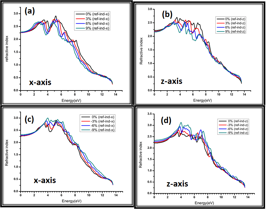
Figure 7: Calculated refractive index for (a) 0%, 3%, 6%, 9% strain along x-axis (b) 0%, 3%, 6%, 9% strain along z-axis (c) 0%, -3%, -6%, -9% strain along x-axis (d) 0%, -3%, -6%, -9% strain along z-axis.
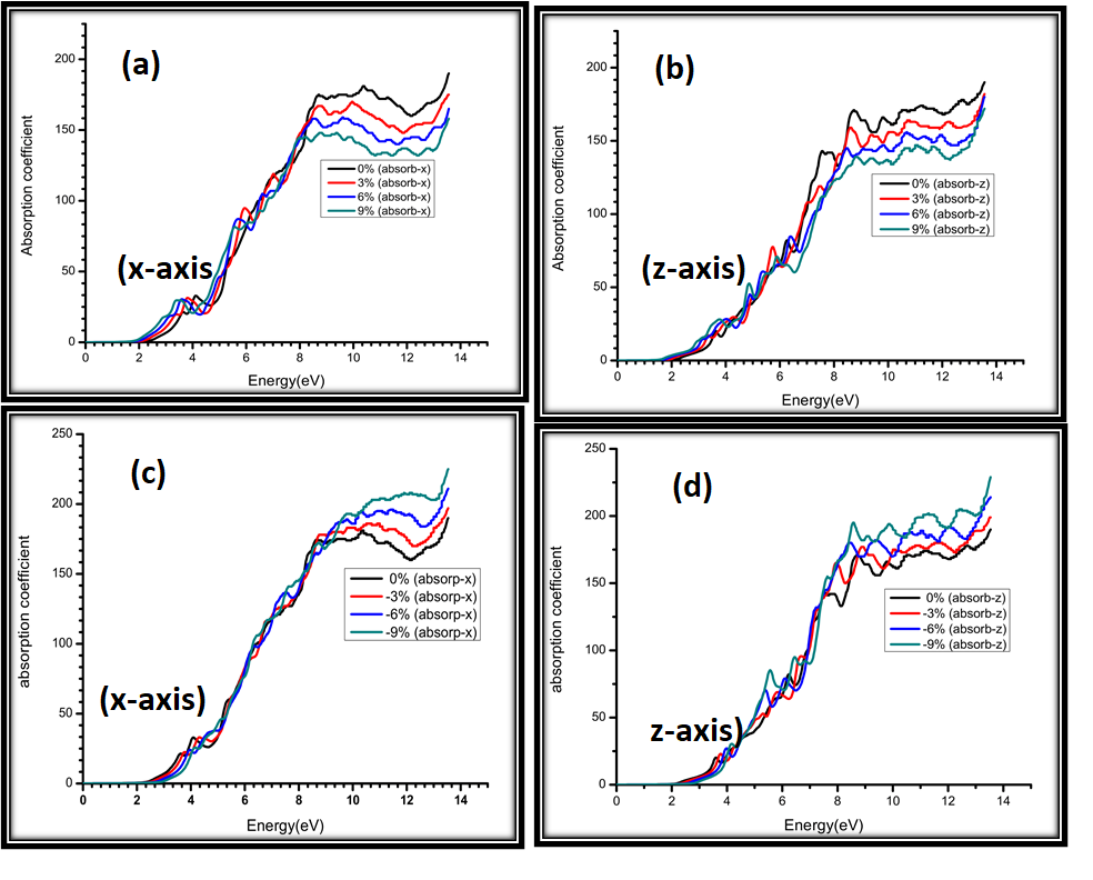
Figure 8: Calculated absorption coefficient for (a) 0%, 3%, 6%, 9% strain along x-axis (b) 0%, 3%, 6%,9% strain along z-axis (c) 0%, -3%, -6%, -9% strain along x-axis (d) 0%, -3%, -6%, -9% strain along z-axis.
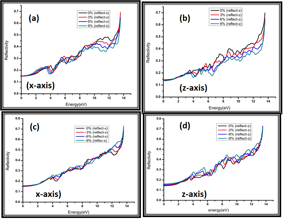
Figure 9: Calculated reflectivity for (a) 0%, 3%, 6%, 9% strain along x-axis (b) 0%, 3%, 6%, 9% strain along z-axis (c) 0%, -3%, -6%, -9% strain along x-axis (d) 0%, -3%, -6%, -9% strain along z-axis.
Figure 8(a) along x-axis shows the absorption coefficient of tensile strained functional absorption coefficient. Figure shows that prominent peak is observed at 8.3 eV. The Figure displays that highest absorption is observed at 0% strain and it decreases as strain increases from 0 to 9%. Along z-axis, Figure 8(a) reveals 0%, 3%, 6% and 9% strain, here the increase in absorption is observed at lower energies, while at higher energies absorption saturates for all the strained and non-strained conditions. For x-axis, however, there was a slight dip in absorption at around 10 eV. For both x-axis and z-axis, Increase in photon energy starts at 2 eV and eventually attains maximum value at about 14 eV (14 eV has an abrupt increase). In Figure 8(c) compressive strain is plotted (0%, -3%, -6% and -9%) along x-axis. Absorption increases upto 10 eV photon energy but afterwards abrupt decrease is observed in absorption at 13 eV for -9%, at 12.8 eV for -6%, at 12.5 eV for -3%, and at 12.2 eV for 0%. In Figure 8(d) along z-axis, when compressive strain is applied to the semiconductor AgGaS2, the absorption increases with increase in the energy and finally saturates before an abrupt increase at 14 eV. When compressive strain is 0%, it absorbs less at similar energy level as compared to 3% strained and -6% strained samples.
Reflectivity against the tensile and compressive strained samples is plotted in Figure 9(a-d). For both x and z-axis, and for both tensile and compressive strains, the reflectivity change with the strain is not significant (it increased form 0.15 to 0.7) for all the energies in the range of 0-14 eV. At 14 eV, however, we did observe a similar sharp rise as for the absorption coefficient. It is important to note that strained and non-strained samples also didn't show a monotonic difference in the reflectivity values. For tensile strained samples, reflectivity was highest for 0% strained samples, while for compressive strained samples, 0% strained sampels had the lowest reflectivity. Overall, we can say that reflectivity-strain relationship is not significant.
In this manuscript, to explore the structural, electronic and optical properties of AgGaS2 under axial strain, Density functional theory (DFT) based Full Potential Linear Augmented Pane Wave (FP-LAPW) method is employed, using Wein2k code. The approximations like PBE-GGA and TB-mBJ potential are used to observe opto-electronic trend under axial strain. When strain applied to AgGaS2 structure, lattice constant variations rise from compressive strain to tensile strain. The calculated results are in reasonable agreement with other theoretical and experimental reports. The band gap varies from 1.645 eV to 2.933 eV which shows that band gap rises from tensile strain to compressive strain, in accordance with calculated total and partial density of states. The dielectric function is used to determine optical properties such as absorption coefficient, refractive index, and reflectivity. Highest absorption is observed at 0% strain while it decrease as strain increases from 0 to 9%. Absorption coefficient rises from tensile strain to compressive strain. In spectrum of reflectivity, no significant variation happens in the visible region with increase in photonic energy. This study has benchmarked various opto-electronic properties under strain conditions, which must be taken into account to understand and utilize in fabricating practical opto-electronic devices for their possible technological applications. We believe results of our study will open new avenues for the applications of AgGaS2.
Heciri, D, Belkhir, H, Belghit, R, Bouhafs, B, Khenata, R & Ahmed, R . 2019. Insight into the structural, elastic and electronic properties of tetragonal inter-alkali metal chalcogenides CsNaX (X = S, Se, and Te) from first-principles calculations. Materials Chemistry and Physics 221:125–137.
Erum, N, Iqbal, A, Iqbal, S S & Nabi, F Un . 2021. Effect of Hydrostatic pressure on structural, electronic, optical and mechanical properties of Lanthanum Oxide (La2O3) Physica scripta 96(11):115702.
Ali, M, Hossain, M A, Rayhan, M, Hossain, M, Uddin, M & Roknuzzaman, M . 2019. First-principles study of elastic, electronic, optical and thermoelectric properties of newly synthesized K2Cu2GeS4 chalcogenide. Journal of Alloys and Compounds 781:37–46.
Omamoke, O E E & Enaroseha, E . 2019. Ab initio investigation of AgGaS2 and AgGaSe2. International Journal of Engineering Applied Sciences and Technology 4(5):354–360.
Hou, H J, Li, T J, Cheng, G, Chen, X L & Xie, L H . 2017. Theoretical study of the structural, elastic and equation of state of chalcopyrite structure AgAlS2. Chalcogenide Letters 14(7):251–257.
Salehi, H & Gordanian, E . 2016. Ab initio study of structural, electronic and optical properties of ternary chalcopyrite semiconductors. Materials Science in Semiconductor Processing 47:51–56.
Li, Y, Lin, J, Fang, Z, Qiu, M, Huang, X, Ding, K, Chen, W & Zhang, Y . 2015. Pressure-tuning the nonlinear-optical properties of AgGaS2 crystal: a first-principle study. Optical Materials Express 5(8):1740.
Erum, N & Iqbal, M A . 2018. Effect of hydrostatic pressure on physical properties of strontium based fluoroperovskites for novel applications. Materials Research Express 5(2):25904.
Iqbal, N Erum ;, Bashir, M A & I . 2021. A DFT study of structural, electronic and optical properties of pristine and intrinsic vacancy defects containing barium zarconate (BaZrO3) using mBJ potential. Physica Scripta 96(2):25807.
Lu, Q, Zhang, H Y, Cheng, Y, Chen, X R & Ji, G F . 2016. Phase transition, elastic and electronic properties of topological insulator Sb2Te3 under pressure: First principle study. Physica B: Condensed Matter 25(2):26401.
Erum, N & Iqbal, M A . 2018. The effect of pressure variation on the elasticity and thermodynamic properties of CaLiF3 for low birefringent lens materials. Chinese Journal of Physics 56(4):353–1361.
Kumar, V, Tripathy, S K & Jha, V . 2012. Second order nonlinear optical properties of AIBIIIC2VI chalcopyrite semiconductors. ” Applied Physics Letters 101(19):192105.
Kopytov, A V & Kosobutsky, A V . 2009. Ab initio calculations of the vibrational spectra of AgInSe2 and AgInTe2. Physics of the Solid State 51(10):2115–2120.
Ullah, S, Din, H U, Murtaza, G, Ouahrani, T, Khenata, R & Omran, S B . 2014. Structural, electronic and optical properties of AgXY2 (X= Al, Ga, in and Y= S, Se, Te) Journal of Alloys and Compounds617:575–583.
Tell, B & Kasper, H . 1971. Optical and Electrical properties of AgGaS2. Physical Review B 4(12):4455–4459.
Catella, G C & Burlage, D . 1998. Crystal Growth and Optical Properties of AgGaS2 and AgGaSe2. MRS Bulletin 23(7):28–36.
Bai, L, Lin, Z, Wang, Z & Chen, C . 2004. Mechanism of Linear and Nonlinear effects of Chalcopyrite AgGaX2 (X=S, Se, Te) crystals. The Journal of Chemical Physics 120(18):8772–8778.
Fox, . 2011. Optical Properties of Solids. New York: Oxford University Press
Dressel, M & Gruner, G . 2002. Electrodynamics of Solids: Optical Properties of Electrons in Matter. UK: Cambridge University Press
Wooten, F . 1972. Optical Properties of Solids. New York: Academic Press
Benkabou, A, Bouafia, H, Sahli, B, Abidri, B, Ameri, M & Hiadsi, S . 2016. Structural, elastic, electronic and thermodynamic investigations of neptunium chalcogenides: First-principles calculations. Journal of Physics: Condensed Matter 54(1):33–41.
Zhang, H, Cheng, Y, Tang, M, Chen, X & Ji, G . 2015. First-principles study of structural, elastic, electronic and thermodynamic properties of topological insulator Sb2Te3 under pressure. Computational Materials Science 96:342–347.
Keywords: AgGaS2,Electrical properties,Optical properties,Strain
Materials Innovations (MI) is an interdisciplinary journal devoted to significant experimental and theoretical findings on the synthesis, structure, charachterization, processing and applications of materials. Materials Innovations is dedicated to publishing peer reviewed novel, cutting edge reports of broad interest to the materials science community.