Materials Innovations
Full Html
Vol 2 Issue 3 (Special Issue)
Bottom-up and Top-down Strategies for Fabrication of Silicon Nanowires
Pages: 69-82
Doi: 10.54738/MI.2022.2302
Doi URL: http://doi.org/10.54738/MI.2022.2302
Ayse Nur Celik 1 , Bilge Tuncel 1 , Nardin Avishan 3 , Syed Nasir Shah?? 4 , Naveed Hussain?? 1
1 Department of Physics, Faculty of Graduate School of Natural and Applied Sciences, Middle East Technical University, Ankara, 06800, Turkey
2 Department of Energy Engineering, Ankara University, Department of Energy Engineering, Ankara University, Ankara, 06560, Turkey
3 Micro and Nanotechnology Program, Graduate School of Natural and Applied Sciences, Middle East Technical University,, Ankara, 06800, Turkey
4 Department of Energy Engineering, Faculty of Mechanical and Aeronautical Engineering , University of Engineering and Technology Taxila, Taxila, Rawalpindi, 47080, Pakistan
5 Department of Electrical Engineering and Computer Sciences, Department of Electrical Engineering and Computer Sciences, University of California, University of California, CA, USA
Silicon (Si) is an important technological material with widespread applications, especially in electronics and optoelectronics. Due to its specific bandgap and low light absorption coefficient, the efficiency of Si-based photodetectors and solar cells is not sufficient for growing industrial needs. By patterning Si into nanowire structures, not only the light-trapping efficiency of the Si can be increased for solar cell and photodetector applications, but the process also imparts other functionalities to nanowires suitable for applications such as antibacterial surfaces, sensing, batteries, etc. Large scale applications of Si nanowires depend on their scalable fabrication. In this article, we summarize the most commonly used fabrication techniques for Si nanowires and discuss their advantages and disadvantages.
Keywords
Silicon, Nanowires, Bottom-up, Growth, Top-down
Silicon is a material that offers qualitative solutions to the recent technical problems of the modern world by its wide spectrum of applications in numerous areas. Especially, in electronic and photovoltaic (PV) industries the strong domination of Si is highly related to its advantageous properties. One of the most important points is its abundance on earth, ensuring the availability of large single crystals with high purity. Besides, having benign thermal and mechanical properties, superior opto-electronic properties of Si provide numerous applications in energy conversion technology. The bandgap of Si, 1.1 eV, matches with the visible spectrum. Thus, it lies in the optimum range in the solar spectra to harvest solar energy. Hence, silicon is the prior element in the photovoltaic industry and 90% of the solar cells employed in solar energy conversion technology are based on Si today.1 However, having indirect bandgap nature which leads to losses in absorption and emission of light is a significant drawback of silicon PVs. Also, relatively low absorption in the solar spectra requires athicker Si layer. Therefore, the optical properties of Si should be improved and this can be accomplished by the implementation? of Si nanostructures.? Similarly,? developments in information technology can be observed by employing materials?that show a high transmission rate and low heat dissipation. These material features can also be realized by Si nanostructures. Silicon nanowires (SiNWs) have been investigated extensively to fabricate high-quality devices by using cost-effective approaches. Research on SiNWs mostly focused on the optimization of the structural properties including ?morphology, size of the wires, or array periodicity. In addition, both theoretical and experimental studies have been carried out on the optical and electrical properties of SiNWs.2 SiNWs have found applications in electronics, photovoltaics, sensing and as antibacterial surfaces.3–6 In traditional Metal-Oxide-Semiconductor Field-Effect-Transistors (MOSFET), SiNWs act as thin channel material. These NW based FETs are excellent candidates for scaling down the transistors, and they also outperform their bulk counterparts in terms of off-state leakage current and drive current generation per device, and low-frequency noise.7,8 In Photovoltaics, due to better light trapping at comparatively lower thickness, and the possibility of making radial p-n junctions not only drastically reduces the cost but also increases the efficiency.9–11

Figure 1: The VLS process for silicon nanowire synthesis.20
The scope and potential of the above-mentioned application of SiNWs depend on the large scale production of high-quality SiNWs. The Quality of SiNWs depends on the methods used for producing SiNWs. Several synthesis methods have been studied for SiNWs fabrication and hence there are various well-established growth techniques that have already been developed. The growth of nanostructures on Si surfaces can be both obtained by bottom-up or top-down deposition techniques. Bottom-up growth techniques are mainly based on vapor-liquid-solid (VLS) mechanism.12 Top-down techniques include various etching techniques including HF etching13, reactive ion etching14,15, laser ablation16, and the Fray-Farthing-Chen-Cambridge (FFC-Cambridge) process17 where electrochemical reduction of SiO2 method is embedded, are most commonly. However, the top-down approaches employed to obtain SiNWs have been found to be more common since bottom-up techniques have some drawbacks such as slow growth rates and relatively high costs. Metal-assisted chemical etching (MACE) is a new innovative technique that is easy, scalable, cost-effective and CMOS compatible.18 metal-assisted chemical etching (MACE) and reactive ion etching (RIE) are more recent and well-established growth techniques. In this review, we will summarize these techniques and will discuss their advantage and disadvantages.
The vapor-liquid-solid growth mechanism of single crystal growth was first mentioned by Wagner and Ellis in their paper of the same name. In this study, they obtained silicon nano-whiskers by VLS growth mechanism.19 In VLS growth, SiNWs are fabricated with the help of a vapor phase precursor and a liquid phase catalyst and directional nucleation of the Si material in the form of wires provided. Therefore, this deposition technique relies on three different stages, namely alloying, nucleation, and wire growth2. The first stage is the formation of metal nanoparticles on a silicon surface. Typically, gold (Au) is used as metal droplets in this process and the formation of Au nanoparticles can be provided by lithography or self-assembly1. During the SiNW growth process, the background Si flux is provided by vapor phase precursor, for instance, silane (SiH4), by using methods such as chemical vapor deposition, electron-beam evaporation, or molecular beam epitaxy. Then, the system is heated up to temperatures above the Au–Si eutectic point. When the supersaturation point of the droplet is reached by the background Si flux, the nucleation of the solid Si in the interface between Si and the droplet starts.17 As a result, the growth of nanowires takes place vertically and the Au droplets are pushed up.1 The VLS growth process is presented schematically in Figure 1.
Silanes and chlorosilanes are the most commonly used Si precursors for VLS growth Si NWs. Chlorosilanes usually crack at higher temperatures so growth will be high temperature (800-1000 oC). As silane usually decomposes at low temperatures, VLS growth can happen at relatively low temperatures (400-600 oC). However, silanes are explosive in nature, so great care needs to be taken while handling these materials.
Au is the most commonly used catalyst due to its easy availability, non-toxicity, and low temperature eutectic with comparably high Si solubility. However, the cost and the fact that Au act as a deep level impurity in the Si can seriously affect the carrier transport of the Si nanowires. In addition to Au, other catalysts such as Ag, Al, Bi, Cd, Co, Cu, Dy, Fe, Mg, Pr, Pt, Ru, Sn, Te, Mn, Ni, Ga, Gd, In, Os, Pb, Pd, Ti, and Zn, can also be used as a catalyst during the VLS process.21–39 Catalysts can be divided into type-A (Au like with single eutectic point), type-B (have much lower solubility of Si and a single eutectic point), and type-C (which are silicide forming metals). The classification of metals is shown in Figure 2. The energy level of Au and other metals catalysts used for the growth of SiNWs and their growth temperatures are given in Figure 3.
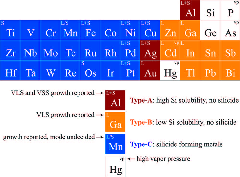
Figure 2: Metals classified based on their phase diagram and their position in the periodic table.21 Adapted with permission from reference 21. Copyright 2018 American Chemical Society.
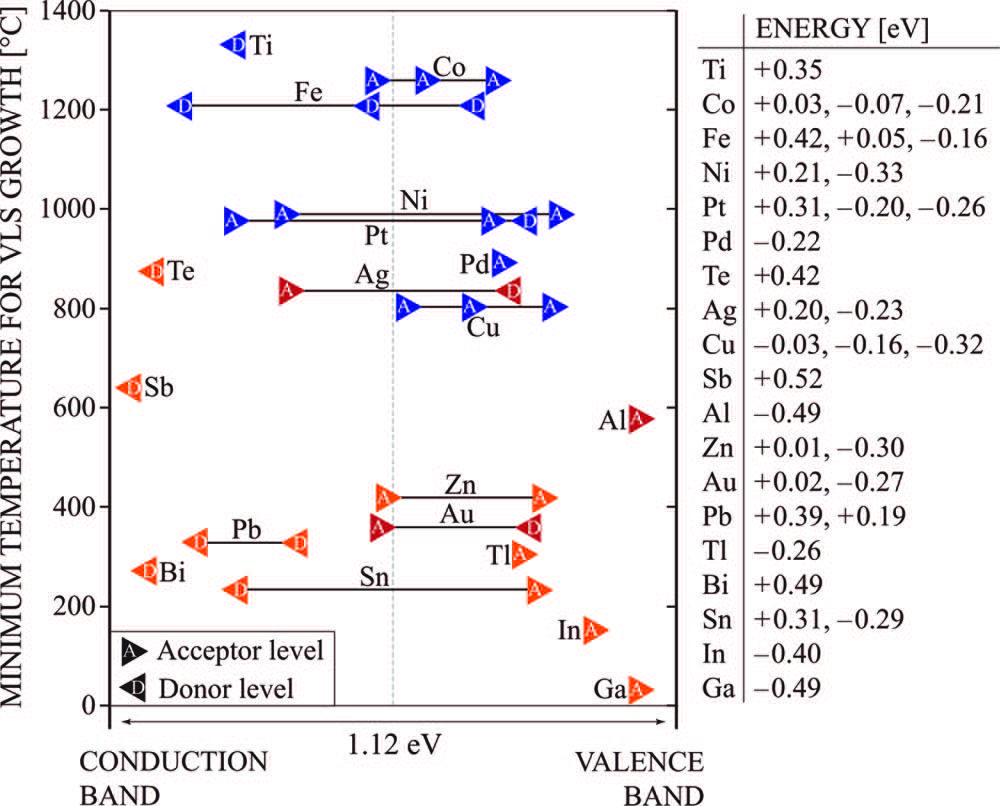
Figure 3: The minimum temperature required for metal catalysts to grow SINWs by vapor-liquid-solid (VLS) method is plotted against their respective impurity energy level in Si.21 The colour codes are adopted from Figure 2: Adapted with permission from reference 21. Copyright 2018 American Chemical Society.
There are multiple VLS techniques, which include high temperature chemical vapor deposition, low-temperature chemical vapor deposition, supercritical-fluid-based, solution-based, molecular beam epitaxy, laser ablation, and silicon monoxide evaporation based. These techniques differ mainly on how the silicon is fed. Si is either fed as elemental Si or a Si compound. Each technique has it advantages and disadvantages, which are discussed elsewhere.21 Chemical vapor deposition is generally the preferred technique, as it offers morphological control, versatility and control over electrical properties. However, issues related to kinking and growth orientation need to be solved.

Figure 4: The top panel shows schematics of RIE process. The bottom panel shows the Influence of over/under passivation and redeposition on etch profile (bottom).40 Adapted with permission from ref 40. Copyright 2018 Elsevier.
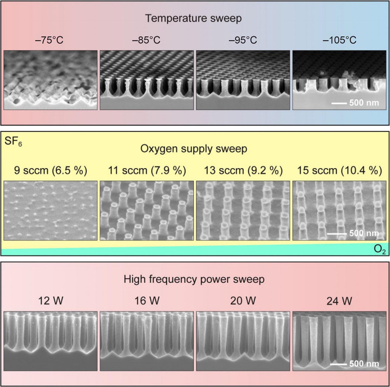
Figure 5: Overview of the effect of etching parameters (temperature, oxygen content, and plate bias) on the morphology of SiNWs.41 Adapted with permission from ref 41. Copyright 2014 Springer.
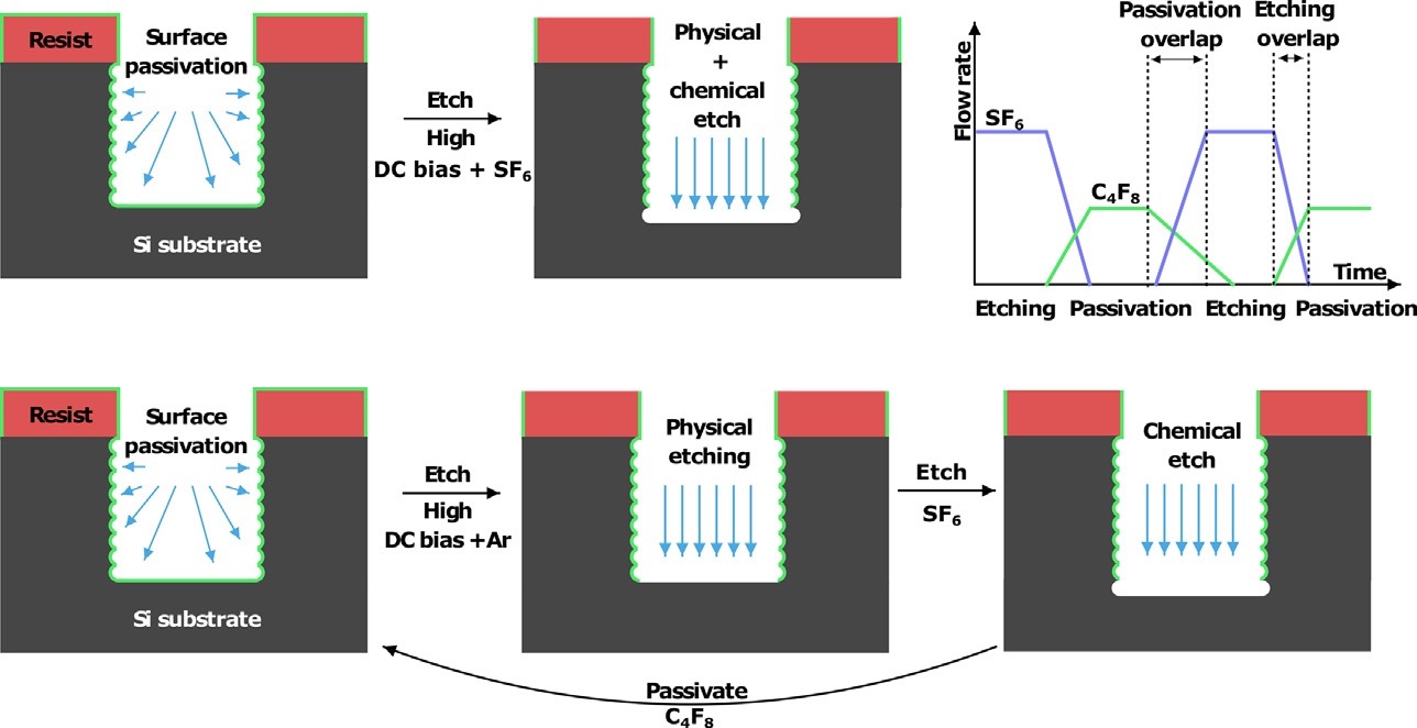
Figure 6: Schematic of a two-step (top) and three-step Bosch etching process (bottom).40 Adapted from ref 40. Copyright 2018 Elsevier.
Reactive ion etching is a top-down approach and perhaps its biggest advantage is its CMOS compatibility. It’s a dry etching technique and is different from chemical etching. It uses chemically reactive plasma to etch Si to obtain desired patterns. A strong radio frequency (RF) electromagnetic field generates the plasma of a reactive gas. Electrons in the plasma are being accelerated and some of the accelerated electrons will sit on Si surface, making it more electron-rich which help attracts the reactive plasma ions to the Si substrate. These plasma ions will react with Si and etch it. Oxygen or halogens (F, Cl, etc.,) are generally used as plasma species and the reactivity of the plasma increases with the electronegativity of these halogens. SF6 or chlorine (Cl2) gas is generally used as a plasma source and C4F8 is used as passivation gas to enhance the anisotropic effect. Once the Si surface is passivated, chemical etching can't take place anymore. To continue the etching process, the bottom surface of the passivated surface is bombarded with energetic ions, which removes the protective passivation layer and allows further chemical etching. To increase the anisotropy, a bias is also applied to Si to direct the ions to the bottom of the sample. During the etching process, by-products will release, which in some cases, redeposit on the Si nanowire, and cause serious morphological changes (Figure 4). Under or over deposition of the passivation layer can also affect the morphology of the SiNWs.
The morphology of SiNWs can be fine-tuned by changing the gas plasma, temperature, substrate bias, flow rate, and plasma power. Figure 5 shows the effect of various parameters or SiNW growth. Details on the effect of these parameters can be found elsewhere.41
In RIE, passivation, physical etching and chemical etching take place at the same time, as shown in Figure 4. A particular example of RIE is deep reactive ion etching (DRIE) or the Bosch process, where passivation, physical, and chemical etching steps take place on a different time scale. DRIE process alternates repeatedly between the etching and passivation process, and involves, physical etching, chemical etching and passivation steps. Bosch process can be two or three-step (Figure 6)
Si, are Ti, Cr, even polystyrene particles42,43 are generally used as masks during the etching. DRIE process allows the fine-tuning of the physical etching process, which does not damage the mask, and hence, SiNWs with better control over diameter can be easily obtained. Generally, DRIE process is suitable for etching long nanowires with a smaller diameter. However, one drawback associated with DRIE is scalloping. Sequential etching and passivation steps give rise to undercuts which is the main reason for scalloping. Scalloping leads to rough surfaces, hence technique is not suitable for applications, where smooth surfaces are required.
To reduce the scalloping, SiNWs of larger diameter are first prepared by the DRIE, and their surface is oxidized. Afterwards, the top SiO2 layer is etched away chemically with HF to produce smoother and lower diameter SiNWs. To further enhance the control over the morphology of SiNWs and achieve smaller diameter SiNWs, DRIE has been coupled with state of the art lithography techniques including UV, electron beam, X-ray and nanoimprint lithography.44–46
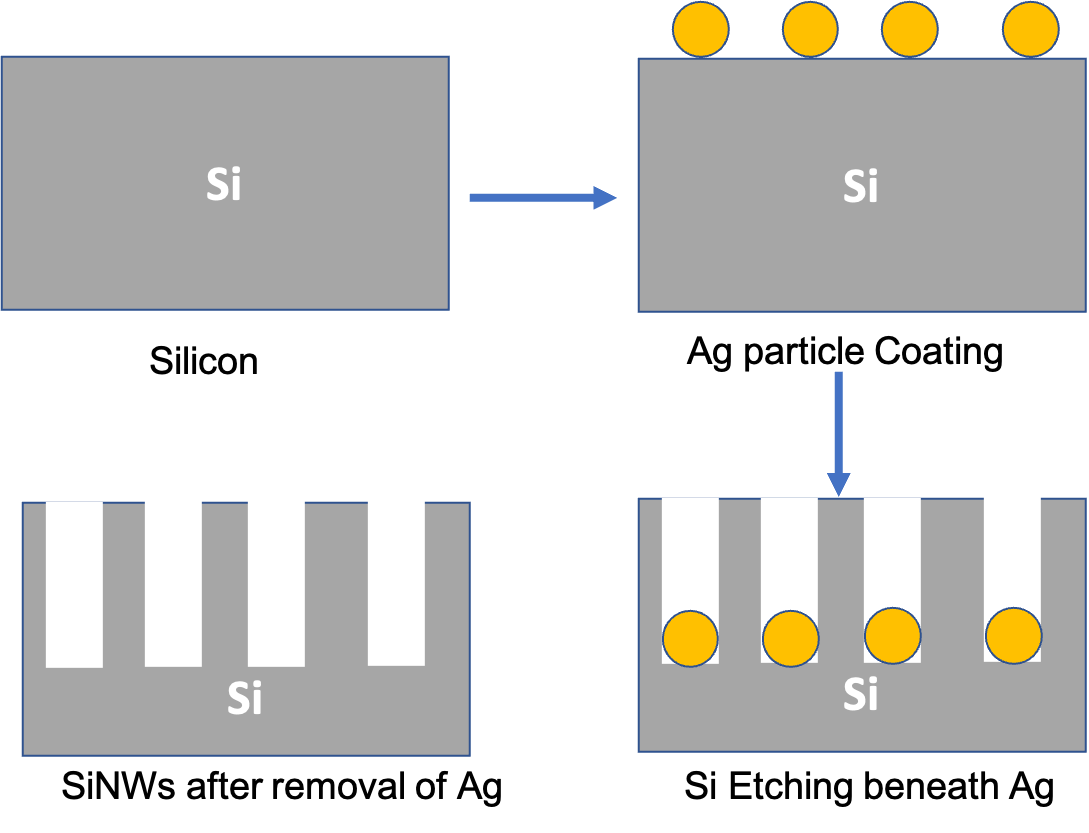
Figure 7: Schematics of MACE fabrication of SiNWs.
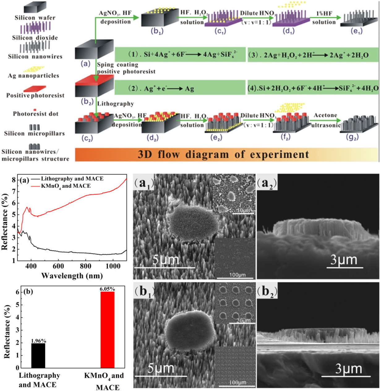
Figure 8: A synthesis scheme, reflectance spectra and SME images of silicon nanowires/micropillars structure fabricated by using lithography and MACE.48 Adapted from ref 48. Copyright 218 Elsevier.
MACE is the wet chemical etching of semiconductors, especially Si, in the presence of metal catalysts. The etching and its effects on the Si substrates are well-known procedures since it is commonly applied in the industrial production of Si-based devices. However, MACE is a relatively new technique, and though it has great potential for its future use in the industry, currently, its applications in the Si etching in the industry are limited. Similar to VLS growth, the MACE process starts with the deposition of the metal nanoparticles on the Si substrate. In addition to Au, silver (Ag) is also one of the most popular material in this stage since both Au and Ag nanoparticles can be grown by a wide range of deposition techniques such as thermal evaporation, sputtering and electron beam evaporation, etc. Other metals that can be used as catalyst include platinum, palladium, aluminum, iron, nickle, and copper. Metals are deposited on the Si surface using variety of methods including sputter deposition, electron beam evaporation, thermal evaporation, electroless deposition, focused ion beam assisted deposition, etc. Some of these methods can be combined with lithography to selectively cover Si regions with the metal. Each method has its own advantages and disadvantages. MACE, besides presenting the simple process, also provides the control over the deposition of catalyst with high precision.
Eelectroless plating is the simplest method employed for MACE process. Si substrate is immersed in HF/noble metal solutions (e.g., AgNO3 or HAuCl4), where deposition and etching happens simultaneously. Metal ions in the solution acquire electrons from the Si valance band and inject holes into the Si. Consequently, metal ions are reduced and deposit on the surface as metal particles, and Si beneath these metal particle is oxidized in the form of SiO or SiO2. Finally, the removal of SiO and SiO2 by HF solution results in the beginning of formation of Si nanowires. Continuous oxidation of the Si under the nanoparticles and removal of the oxide layers by HF solution leads to the sinking of the metal nanoparticles to the deeper level of the Si substrate (Figure 7). As a result, final structure contains SiNWs on the surface and metal nanoparticles embedded between them17.
Though, the light trapping efficiency of SiNWs fabricated using MACE is excellent, but the control over shape, density and regularity is poor. Si micropillars fabricated using more common lithography methods have excellent control over morphology, but their light-trapping efficiency is not good.47 A combination of MACE with lithography can produce SiNWs with great control over the morphology as well as good light-trapping efficiency. Xi et al.48 have demonstrated a facile synthesis of SiNWs/SiMPs using lithography and MACE, where they first spin-coated and baked a photoresist on the Si wafers. Photoresist dots of 5um diameter were obtained by exposing the photoresist for 90-100 s and subsequent development in solvent for 40-50 seconds, and then MACE method was used to grow SiNWs/SiMPs. As can be seen in SEM image of Figure 8, SiNWs/SiMPs structures were very well arranged and also showed the better light trapping efficiency.
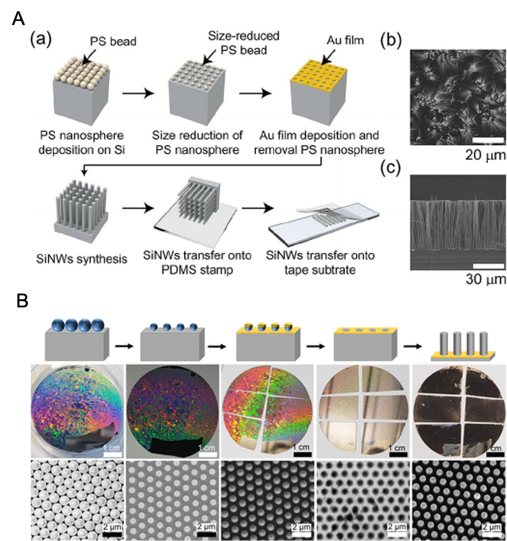
Figure 9: (A) (a) Schematic of MACE SiNW fabrication with Nanosphere Lithography. (b, c) SEM top and cross-sectional image of SiNWs, respectively.51 Adapted from ref 52. Copyright 2015 IEEE. (B) Synthesis of SiNW arrays using the combination of MACE and colloidal lithography. The top row shows the schematics of steps involved in fabrication. The middle row shows the photographs of 2″ Si wafers during the process. Bottom row: SEM images at every step in top row.52 Adapted with permission from ref 52. Copyright 2020 American Chemical Society.
MACE can be used in tandem with colloidal lithography for the production of large-scale homogeneous SiNW arrays (Figure 9).49,50 Colloidal lithography is not only simple but also a very cost-effective approach for fabricating SiNW arrays with precise control over the geometry without requiring expensive and sophisticated nanopatterning techniques. It involves the monolayer deposition of the colloidal spheres (polystyrene or core core-shell SiO2 particles), with controllable size (plasma etching is used to shrink the particles) and dispersion.51 While the colloidal mask can be fabricated by a variety of methods (drop-casting, spin-coating, etc,) large-scale and good quality monolayers without macroscopic defects can be only be grown by self-assembly on the water-air interface, ideally by using a Langmuir trough. This colloidal monolayer act as a template for metal deposition. After the lift-off process metal nanohole arrays are obtained which are used for subsequent MACE etching. Thus, the combination of colloidal lithography and MACE provides a benchtop, cost-effective, and versatile way to synthesize SiNW arrays with tuneable geometries. Grain boundaries and other defects on the colloidal particles can affect the final quality of the SiNWs.
Fabricated SiNWs can be further processed to tailor their properties for any specific applications. For example, bisegmented and graded arrays have been fabricated from MACE synthesiszed NW arrays.53 As shown in Figure 10, synthesized NW arrays were dipped into KOH solution to thin down the diameter of NWs by etching. A further MACE step grew thicker NWs at the bottom. Diameter The diameter of the top segment depended on the KOH etching, while the diameter of the bottom segment was dependent on the colloidal template. While the single-diameter NWs show a single sharp dip in their reflectance spectrum, the bisegmented NWs shows a significantly broadened reflectance dip. As can be seen for the absorption maps, the bottom large diameter segment absorbs more at longer wavelengths, while the top smaller diameter section absorbs more at shorter wavelengths. This combination is responsible for a broader dip in the reflection spectrum of bisegmented NWs.

Figure 10: (a) Schematic of the synthesis of bisegmented SINW using sequential MACE and KOH etching steps. (b) Secondary electron SEM image of bisegmented SiNWs. (c, d) Measured and simulated reflectance spectra of two different and bisgemented NWs, respectively. (e) Two-dimensional maps of the simulated relative absorption of bisegmented SiNWs at 553 and 638 nm.53 Adapted with permission from ref 53. Copyright 2020 American Chemical Society.
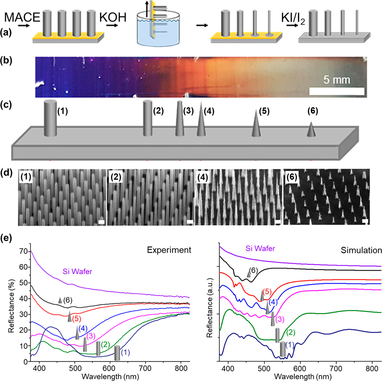
Figure 11: (a) Schematics showing the dip-etching process to fabricate gradient SiNWs (b) Optical image of a gradient SiNW sample. (c, d) Scheme of the gradient morphology at various positions indicated with numbers and corresponding electron SEM images at those positions. (e) Measured and simulated reflectance spectra for different positions on the SiNW structure.53 Adapted with permission from ref 53. Copyright 2020 American Chemical Society.
The same group fabricated graded NW arrays by dipping the MACE fabricated NWs into a two-phase mixture of KOH at the bottom and hexane at the top, see Figure 11. Progressive removal of the substrate from the solution leads to a gradual change of the NW diameter, which is also depicted by the change in colour from blue to grey. Change of colour is also reflected in the UV-Vis reflectance spectra. For homogeneous etching, hexane is used to reduce the residual KOH adhering to the SiNW substrate.
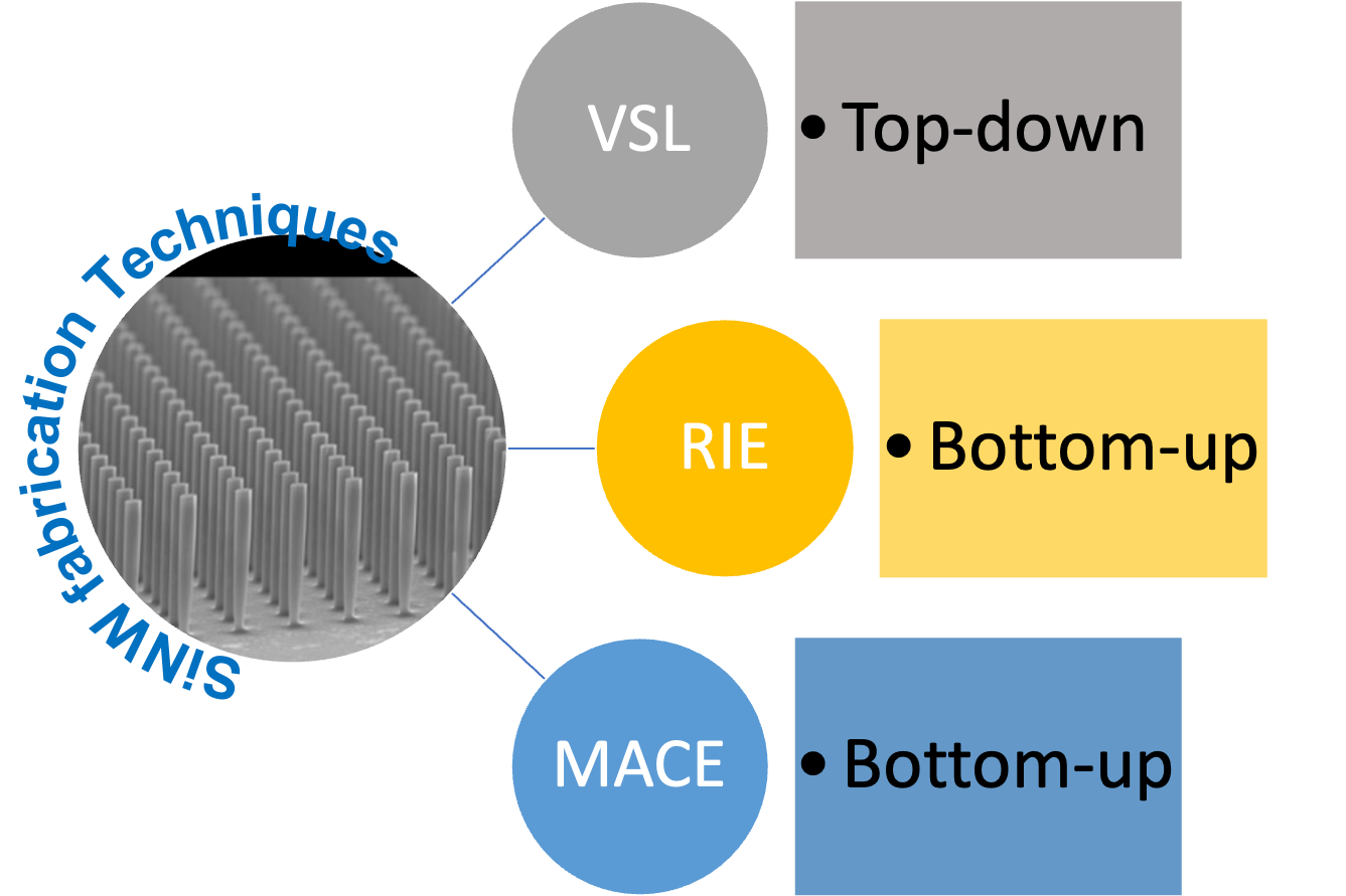
Figure 12: Summary of SiNW fabrication techniques
We have summarized VSL, RIE and MACE techniques for the fabrication of SiNWs (Figure 12). VLS mechanism is not only applicable to Si but also to a range of other materials. It is a bottom-up approach to grow SiNWs. CVD technique is the best technique to grow SiNWs via the VSL method as it offers better control over morphology and electrical properties. RIE and MACE are bottom-up approaches. Since bulk Si is used as the initial material range of SiNW shapes and morphologies can be carved into the bulk Si, a benefit not associated with bottom-up methods. Moreover, post-SiNW fabrication, leftover bulk SiI can also be used depending upon the requirement of the application. RIE is a well-matured CMOS process, so, SiNW fabricated with RIE can be integrated with Si devices easily. Moreover, DRIE coupled with advanced lithographic techniques allows the fabrication of long nanowires with thin diameters. MACE is a simple, innovative and cost-effective new technique for the fabrication of large scale and integration with the CMOS process. Due to the inherent simplicity of the process, by tuning different parameters, gradient and bisegment SiNWs can also be fabricated easily. MACE can also work together with advanced lithographic techniques to give better control over size and morphology. Lesson learnt from different techniques, with a combination of different growth techniques, and coupling these fabrication techniques with advanced lithographic methods can open the way for large scale, cost-effective and high-quality SiNW growth for large scale applications such as solar cells, sensors, etc.
Apart from the techniques mentioned in this review article, there are also other less commonly fabrication techniques. For example, laser beam ablation, ion beam etching, thermal evaporation oxide-assisted growth are the top-down synthesis methods. While, molecular beam epitaxy and precipitation from solution are the examples of bottom-up strategies.
This publication/paper has been produced benefiting from the 2232 International Fellowship for Outstanding Researchers Program of TÜBITAK (Project No: 118C214). However, the entire responsibility of the publication/paper belongs to the owner of the publication/paper. The financial support received from TÜBITAK does not mean that the content of the publication is approved in a scientific sense by TÜBITAK.
Priolo, Francesco, Gregorkiewicz, Tom, Galli, Matteo & Krauss, Thomas F. . 2014. Silicon nanostructures for photonics and photovoltaics. Nature Nanotechnology 9(1):19–32.
Yu, Peng, Wu, Jiang, Liu, Shenting, Xiong, Jie, Jagadish, Chennupati & Wang, Zhiming M. . 2016. Design and fabrication of silicon nanowires towards efficient solar cells. Nano Today 11(6):704–737.
Zhou, X.T., Hu, J.Q., Li, C.P., Ma, D.D.D., Lee, C.S. & Lee, S.T. . 2003. Silicon nanowires as chemical sensors. Chemical Physics Letters 369(1-2):220–224.
Yu, Peng, Wu, Jiang, Liu, Shenting, Xiong, Jie, Jagadish, Chennupati & Wang, Zhiming M. . 2016. Design and fabrication of silicon nanowires towards efficient solar cells. Nano Today 11(6):704–737.
Susarrey-Arce, A., Sorzabal-Bellido, I., Oknianska, A., McBride, F., Beckett, A. J., Gardeniers, J. G. E., Raval, R., Tiggelaar, R. M. & Diaz Fernandez, Y. A. . 2016. Bacterial viability on chemically modified silicon nanowire arrays. Journal of Materials Chemistry B 4(18):3104–3112.
Goldberger, Josh, Hochbaum, Allon I., Fan, Rong & Yang, Peidong . 2006. Silicon Vertically Integrated Nanowire Field Effect Transistors. Nano Letters 6(5):973–977.
Goldberger, Josh, Hochbaum, Allon I., Fan, Rong & Yang, Peidong . 2006. Silicon Vertically Integrated Nanowire Field Effect Transistors. Nano Letters 6(5):973–977.
Fahad, Hossain M. & Hussain, Muhammad M. . 2012. Are Nanotube Architectures More Advantageous Than Nanowire Architectures For Field Effect Transistors? Scientific Reports 2(1):1–7.
Seo, Myunghae, Yoon, Sol, Cho, Hyeonsu, Lee, Seungho, Kim, Kihyun, Kong, Byoung Don, Meyyappan, Meyya & Baek, Chang-Ki . 2020. Solar Cell Using Hourglass-Shaped Silicon Nanowires for Increased Light-Trapping Path. IEEE Journal of Photovoltaics 10(2):475–479.
Jia, Guobin, Gawlik, Annett, Bergmann, Joachim, Eisenhawer, Bjorn, Schonherr, Sven, Andra, Gudrun & Falk, Fritz . 2014. Silicon Nanowire Solar Cells With Radial p-n Heterojunction on Crystalline Silicon Thin Films: Light Trapping Properties. IEEE Journal of Photovoltaics 4(1):28–32.
Garnett, Erik & Yang, Peidong . 2010. Light Trapping in Silicon Nanowire Solar Cells. Nano Letters 10(3):1082–1087.
Gunawan, Oki & Guha, Supratik . 2009. Characteristics of vapor–liquid–solid grown silicon nanowire solar cells. Solar Energy Materials and Solar Cells 93(8):1388–1393.
Kato, Yuki & Adachi, Sadao . 2011. Synthesis of Si Nanowire Arrays in AgO/HF Solution and Their Optical and Wettability Properties. Journal of The Electrochemical Society 158(7):K157–K163.
Fu, Y. Q., Colli, A., Fasoli, A., Luo, J. K., Flewitt, A. J., Ferrari, A. C. & Milne, W. I. . 2009. Deep reactive ion etching as a tool for nanostructure fabrication. Journal of Vacuum Science & Technology B: Microelectronics and Nanometer Structures 27(3):1520.
Chen, Yi, Xu, Zhida, Gartia, Manas R., Whitlock, Daren, Lian, Yaguang & Liu, G. Logan . 2011. Ultrahigh Throughput Silicon Nanomanufacturing by Simultaneous Reactive Ion Synthesis and Etching. ACS Nano 5(10):8002–8012.
Zhang, Y. F., Tang, Y. H., Wang, N., Yu, D. P., Lee, C. S., Bello, I. & Lee, S. T. . 1998. Silicon nanowires prepared by laser ablation at high temperature. Applied Physics Letters 72(15):1835–1837.
Liu, Xiaogang, Coxon, Paul R., Peters, Marius, Hoex, Bram, Cole, Jacqueline M. & Fray, Derek J. . 2014. Black silicon: fabrication methods, properties and solar energy applications. Energy Environ. Sci. 7(10):3223–3263.
Huang, Zhipeng, Geyer, Nadine, Werner, Peter, de Boor, Johannes & Gösele, Ulrich . 2011. Metal-Assisted Chemical Etching of Silicon: A Review. Advanced Materials 23(2):285–308.
Wagner, R. S. & Ellis, W. C. . 1964. VAPOR?LIQUID?SOLID MECHANISM OF SINGLE CRYSTAL GROWTH. Applied Physics Letters 4(5):89–90.
Englander, O . 2005. Localized Synthesis, Assembly and Integration of Silicon Nanowires.
Schmidt, V., Wittemann, J. V. & Gösele, U. . 2010. Growth, Thermodynamics, and Electrical Properties of Silicon Nanowires. Chemical Reviews 110(1):361–388.
Chung, Sung-Wook, Yu, Jae-Young & Heath, James R. . 2000. Silicon nanowire devices. Applied Physics Letters 76(15):2068–2070.
Yang, Yi-Han, Wu, Sheng-Jia, Chiu, Hui-Shan, Lin, Ping-I & Chen, Yit-Tsong . 2004. Catalytic Growth of Silicon Nanowires Assisted by Laser Ablation. The Journal of Physical Chemistry B 108(3):846–852.
Koren, E., Elias, G., Boag, A., Hemesath, E. R., Lauhon, L. J. & Rosenwaks, Y. . 2011. Direct Measurement of Individual Deep Traps in Single Silicon Nanowires. Nano Letters 11(6):2499–2502.
Nebol'sin, V. A., Shchetinin, A. A., Dolgachev, A. A. & Korneeva, V. V. . 2005. Effect of the Nature of the Metal Solvent on the Vapor-Liquid-Solid Growth Rate of Silicon Whiskers. Inorganic Materials 41(12):1256–1259.
Sharma, S, Kamins, T.I & Williams, R.Stanley . 2004. Diameter control of Ti-catalyzed silicon nanowires. Journal of Crystal Growth 267(3-4):613–618.
Uesawa, Norihisa, Inasawa, Susumu, Tsuji, Yoshiko & Yamaguchi, Yukio . 2010. Gas-Phase Synthesis of Rough Silicon Nanowires via the Zinc Reduction of Silicon Tetrachloride. The Journal of Physical Chemistry C 114(10):4291–4296.
Yang, Yi-Han, Wu, Sheng-Jia, Chiu, Hui-Shan, Lin, Ping-I & Chen, Yit-Tsong . 2004. Catalytic Growth of Silicon Nanowires Assisted by Laser Ablation. The Journal of Physical Chemistry B 108(3):846–852.
Givargizov, E I . 1975. FUNDAMENTAL ASPECTS OF VLS GROWTH. Vapour Growth and Epitaxy 20–30.
Wagner, R. S., Ellis, W. C., Jackson, K. A. & Arnold, S. M. . 1964. Study of the Filamentary Growth of Silicon Crystals from the Vapor. Journal of Applied Physics 35(10):2993–3000.
Iacopi, F, Vereecken, P M, Schaekers, M, Caymax, M, Moelans, N, Blanpain, B, Richard, O, Detavernier, C & Griffiths, H . 2007. Plasma-enhanced chemical vapour deposition growth of Si nanowires with low melting point metal catalysts: an effective alternative to Au-mediated growth. Nanotechnology 18(50):505307.
Wagner, R. S., Ellis, W. C., Jackson, K. A. & Arnold, S. M. . 1964. Study of the Filamentary Growth of Silicon Crystals from the Vapor. Journal of Applied Physics 35(10):2993–3000.
Sunkara, M. K., Sharma, S., Miranda, R., Lian, G. & Dickey, E. C. . 2001. Bulk synthesis of silicon nanowires using a low-temperature vapor–liquid–solid method. Applied Physics Letters 79(10):1546–1548.
Schmidt, Volker, Senz, Stephan & Gösele, Ulrich . 2005. UHV chemical vapour deposition of silicon nanowires. Zeitschrift für Metallkunde 96(5):427–428.
Kayes, Brendan M., Filler, Michael A., Putnam, Morgan C., Kelzenberg, Michael D., Lewis, Nathan S. & Atwater, Harry A. . 2007. Growth of vertically aligned Si wire arrays over large areas (>1cm2) with Au and Cu catalysts. Applied Physics Letters 91(10):103110.
Wagner, R. S., Ellis, W. C., Jackson, K. A. & Arnold, S. M. . 1964. Study of the Filamentary Growth of Silicon Crystals from the Vapor. Journal of Applied Physics 35(10):2993–3000.
Wagner, R. S. & Ellis, W. C. . 1964. VAPOR?LIQUID?SOLID MECHANISM OF SINGLE CRYSTAL GROWTH. Applied Physics Letters 4(5):89–90.
Heitsch, Andrew T., Fanfair, Dayne D., Tuan, Hsing-Yu & Korgel, Brian A. . 2008. Solution−Liquid−Solid (SLS) Growth of Silicon Nanowires. Journal of the American Chemical Society 130(16):5436–5437.
Nebol’sin, V A & Shchetinin, A A . 2003. Role of Surface Energy in the Vapor-Liquid-Solid Growth of Silicon. Inorganic materials 39(9):899–903.
Solanki, Amit & Um, Handon . 2018. Top-Down Etching of Si Nanowires. Semiconductors and Semimetals 98:71–149.
Merzsch, S., Steib, F., Wasisto, H. S., Stranz, A., Hinze, P., Weimann, T., Peiner, E. & Waag, A. . 2014. Production of vertical nanowire resonators by cryogenic-ICP–DRIE. Microsystem Technologies 20(4-5):759–767.
Garnett, Erik & Yang, Peidong . 2010. Light Trapping in Silicon Nanowire Solar Cells. Nano Letters 10(3):1082–1087.
Jansen, Henri, Gardeniers, Han, Boer, Meint de, Elwenspoek, Miko & Fluitman, Jan . 1996. A survey on the reactive ion etching of silicon in microtechnology. Journal of Micromechanics and Microengineering 6(1):14–28.
Chou, Stephen Y., Krauss, Peter R. & Renstrom, Preston J. . 1996. Imprint Lithography with 25-Nanometer Resolution. Science 272(5258):85–87.
Vieu, C., Carcenac, F., Pépin, A., Chen, Y., Mejias, M., Lebib, A., Manin-Ferlazzo, L., Couraud, L. & Launois, H. . 2000. Electron beam lithography: resolution limits and applications. Applied Surface Science 164(1-4):111–117.
Gates, Byron D., Xu, Qiaobing, Stewart, Michael, Ryan, Declan, Willson, C. Grant & Whitesides, George M. . 2005. New Approaches to Nanofabrication: Molding, Printing, and Other Techniques. ChemInform 36(27):1171–1196.
Fan, Zhiqiang, Zhang, Weijia, Fu, Yaolong, Yan, Lanqin & Ma, Xiaobo . 2016. Facile Synthesis of Silicon Micropillar Arrays Using Extreme Ultraviolet Lithography and Ag-Assisted Chemical Etching Method. The Journal of Physical Chemistry C 120(12):6824–6834.
Xi, Yilian, Zhang, Weijia, Fan, Zhiqiang, Ma, Qiang, Wang, Shan, Ma, Denghao, Jiang, Zhaoyi, Li, Hongzhen & Zhang, Yulong . 2018. A facile synthesis of silicon nanowires/micropillars structure using lithography and metal-assisted chemical etching method. Journal of Solid State Chemistry 258:181–190.
Wendisch, Fedja J., Oberreiter, Richard, Salihovic, Miralem, Elsaesser, Michael S. & Bourret, Gilles R. . 2017. Confined Etching within 2D and 3D Colloidal Crystals for Tunable Nanostructured Templates: Local Environment Matters. ACS Applied Materials & Interfaces 9(4):3931–3939.
Wendisch, Fedja J., Oberreiter, Richard, Salihovic, Miralem, Elsaesser, Michael S. & Bourret, Gilles R. . 2017. Confined Etching within 2D and 3D Colloidal Crystals for Tunable Nanostructured Templates: Local Environment Matters. ACS Applied Materials & Interfaces 9(4):3931–3939.
In, Chihun, Seo, Jungmok, Kwon, Hyukho, Choi, Jeongmook, Sim, Sangwan, Kim, Jaeseok, Kim, Taeyong, Lee, Taeyoon & Choi, Hyunyong . 2015. Counterbalanced Effect of Surface Trap and Auger Recombination on the Transverse Terahertz Carrier Dynamics in Silicon Nanowires. IEEE Transactions on Terahertz Science and Technology 5(4):605–612.
Wendisch, Fedja J., Rey, Marcel, Vogel, Nicolas & Bourret, Gilles R. . 2020. Large-Scale Synthesis of Highly Uniform Silicon Nanowire Arrays Using Metal-Assisted Chemical Etching. Chemistry of Materials 32(21):9425–9434.
Wendisch, Fedja J., Abazari, Mehri, Mahdavi, Hossein, Rey, Marcel, Vogel, Nicolas, Musso, Maurizio, Diwald, Oliver & Bourret, Gilles R. . 2020. Morphology-Graded Silicon Nanowire Arrays via Chemical Etching: Engineering Optical Properties at the Nanoscale and Macroscale. ACS Applied Materials & Interfaces 12(11):13140–13147.
Keywords: Silicon, Nanowires, Bottom-up, Growth, Top-down
Materials Innovations (MI) is an interdisciplinary journal devoted to significant experimental and theoretical findings on the synthesis, structure, charachterization, processing and applications of materials. Materials Innovations is dedicated to publishing peer reviewed novel, cutting edge reports of broad interest to the materials science community.